
Unlocking VLSI Reliability: A Deep Dive into Advanced Design for Testability (DFT)
Mastering the intricacies of modern chip design through cutting-edge test methodologies for enhanced quality and efficiency.
Key Insights into Advanced DFT for VLSI
- Comprehensive Testability: Advanced DFT techniques are indispensable for ensuring the quality and reliability of complex Very Large Scale Integration (VLSI) designs, especially System-on-Chips (SoCs) with billions of transistors.
- Efficiency and Cost Savings: By integrating testability features directly into the chip, DFT significantly reduces testing time, lowers overall costs, and accelerates time-to-market by catching flaws early in the design cycle.
- Diverse Methodologies: Modern DFT employs a synergistic blend of techniques such as optimized Scan Chains, Built-In Self-Test (BIST), Automatic Test Pattern Generation (ATPG) with compression, and Boundary Scan (JTAG) to achieve high fault coverage and efficient fault diagnosis.
As integrated circuits (ICs) continue their relentless march towards greater complexity, integrating billions of transistors onto a single silicon die, the challenge of ensuring their flawless operation becomes increasingly formidable. This is where Advanced Design for Testability (DFT) techniques emerge as paramount. DFT is not merely an afterthought in the design process; it is a proactive and integral methodology that imbues chips with the inherent ability to test themselves efficiently, pinpointing defects with precision, and ultimately guaranteeing the high quality and reliability expected in today's sophisticated electronic systems.
The core objective of advanced DFT is to enhance both the observability (the ability to monitor internal circuit states) and controllability (the ability to set specific internal states) of an IC. Without these built-in test features, the sheer scale and intricate nature of modern VLSI designs would render traditional external testing approaches prohibitively time-consuming, expensive, and often outright infeasible. By baking testability into the design from the ground up, DFT transforms the daunting task of fault detection and diagnosis into a manageable, automated process, leading to substantial cost and time savings across the entire product lifecycle.
An image illustrating the importance of intelligent DFT chip architecture for accelerated success.
The Imperative of DFT in Modern VLSI Design
The growing complexity of VLSI designs, driven by smaller process nodes and advanced System-on-Chip (SoC) architectures, necessitates robust DFT strategies. These chips power everything from smartphones to artificial intelligence accelerators, and any defect can lead to significant financial losses, reputational damage, and even safety concerns. DFT addresses these challenges by ensuring that even the most intricate internal logic can be thoroughly verified.
Strategic Advantages of Integrating DFT
- Reduced Test Costs and Time: By enabling early fault detection and automation, DFT minimizes reliance on expensive external test equipment and dramatically shortens the time required for testing, validation, and debugging. This directly translates to lower manufacturing costs and improved profitability.
- Enhanced Product Quality and Reliability: Effective DFT identifies and rectifies design flaws and manufacturing defects early, leading to higher manufacturing yields and more reliable Application-Specific Integrated Circuits (ASICs). Chips reaching the market are of higher quality, reducing field failures and warranty claims.
- Accelerated Time-to-Market: Streamlined testing and validation processes, facilitated by DFT, expedite product development cycles. This allows companies to introduce their VLSI products to the market faster, gaining a crucial competitive edge.
- Improved Fault Coverage and Diagnosis: DFT techniques significantly increase the ability to detect various fault types, including stuck-at, transition, and bridging faults. They also simplify the diagnostic process, enabling engineers to pinpoint the exact location of defects quickly and accurately.
Pivotal Advanced DFT Techniques for VLSI
Modern VLSI chips demand sophisticated DFT techniques that go beyond basic test methods. These advanced approaches are continuously evolving, leveraging innovations in Electronic Design Automation (EDA) tools and design methodologies to meet the stringent requirements of today's semiconductor industry.
Scan Chain Insertion and Optimization
Scan chain insertion is a cornerstone of modern DFT. This technique transforms sequential elements, such as flip-flops, into serial shift registers in a special "test mode." This allows test patterns to be shifted in and out, providing direct control and observation of internal circuit states. Advanced aspects of scan chains include:
Scan Compression/Decompression:
To handle the vast volume of test data in complex designs, compression and decompression algorithms are employed. These reduce the size of test patterns and the number of scan pins required, minimizing tester memory and test application time.Hierarchical Scan Design:
For large System-on-Chips (SoCs), designs are divided into smaller, manageable blocks, each with its own scan chains. These are then integrated at the top level, simplifying the overall test process.Timing-Aware Scan Insertion:
Ensures that the addition of scan chains does not introduce unwanted delay paths that could negatively impact the chip's operational frequency (timing closure).Multi-Domain Scan Chains:
In multi-core SoCs, different cores can be tested independently, reducing test time and complexity.Scan Chain Optimization:
Techniques like scan reordering and stitching optimize the physical layout of scan chains to minimize interconnect wires and improve routing efficiency, particularly when dealing with clock mixing and internal clock domains.
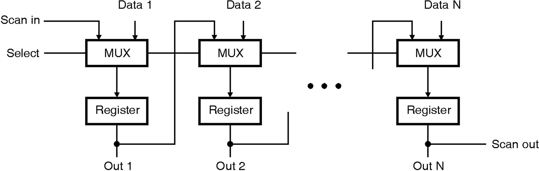
A visual representation of scan path testing, illustrating how internal flip-flops are connected into a serial chain for testability.
Built-In Self-Test (BIST) Architectures
BIST enables the chip to test itself, significantly reducing reliance on expensive external Automated Test Equipment (ATE). This is achieved by embedding test pattern generators (e.g., Linear Feedback Shift Registers - LFSRs) and output response analyzers (e.g., Multiple-Input Signature Registers - MISRs) directly onto the chip. Key BIST types include:
Memory BIST (MBIST):
Specifically designed for testing embedded memory blocks (SRAM, DRAM, etc.) that are ubiquitous in modern SoCs. MBIST automates the complex test algorithms required for memory arrays, detecting faults like stuck-at, transition, and address decoder faults.Logic BIST (LBIST):
Used for testing large logic blocks within the chip. Advanced LBIST focuses on achieving high fault coverage with low-power test operation and minimal test time.At-Speed Testing:
BIST facilitates testing at the actual operational frequency of the IC, crucial for detecting timing-related defects that might otherwise go unnoticed.
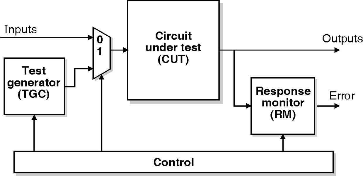
Diagram illustrating the fundamental components of a Built-in Self-Test (BIST) architecture within an integrated circuit.
Automatic Test Pattern Generation (ATPG)
ATPG is a software-driven process that generates optimal test patterns (vectors) to detect specific fault models within digital circuits. Advanced ATPG algorithms are critical for achieving high fault coverage in complex designs.
Compression-Aware ATPG:
Integrates seamlessly with scan compression techniques, optimizing test pattern generation to work with the on-chip decompression logic, thereby reducing test data volume.Hierarchical ATPG:
For complex SoCs, ATPG can be applied hierarchically to individual blocks before being integrated at the top level, managing complexity and reducing computation time.Low-Power ATPG:
Generates test patterns that minimize peak and average power consumption during testing, preventing chip damage and excessive heat.Fault Models and Analysis:
Advanced ATPG considers various fault models (stuck-at, transition, bridging) and uses sophisticated fault simulation to ensure comprehensive fault coverage and accurate diagnosis.
Boundary Scan Testing (IEEE 1149.1 Standard - JTAG)
Boundary Scan, standardized as IEEE 1149.1 (JTAG), is essential for testing interconnects between ICs on a Printed Circuit Board (PCB). It involves adding boundary scan cells around the periphery of the chip's I/O pins, which can be configured into a scan chain.
Board-Level and Intra-Chip Testing:
JTAG simplifies testing of connections between chips without physical probes and extends to testing internal buses and interfaces within complex SoCs.Enhanced Debug Capabilities:
Provides non-intrusive access to internal nodes, significantly aiding in debugging and fault isolation at both chip and board levels.Advanced Extensions:
Newer standards like IEEE 1149.6 address testing of AC-coupled interconnections, further expanding JTAG's utility.
Test Data Compression and Decompression
The exponential growth of test data in VLSI designs necessitates robust compression techniques. These methods reduce the volume of data that needs to be stored and transferred, thereby cutting down test costs and time.
On-Chip Decompression:
Embedded decompressors within the chip receive compressed test patterns and expand them into full-length test vectors internally.Response Compaction:
Reduces the size of the output data generated by the chip during testing while preserving diagnosability. Techniques include signature analysis and X-compaction.Algorithms:
Various algorithms such as dictionary-based, run-length encoding, and statistical coding are employed for efficient data compression.
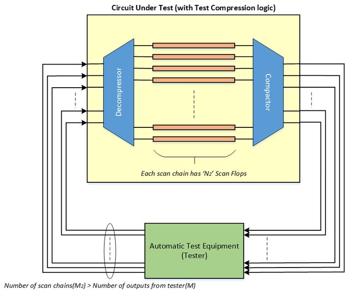
An illustration showing how scan compression techniques reduce the volume of test data, making testing more efficient.
Hierarchical DFT and Compression-Aware Architectures
For highly complex SoC designs, a hierarchical DFT approach is crucial. This involves implementing DFT at the module or core level first and then integrating these sub-infrastructures at the top level. This approach facilitates design reuse and manages complexity effectively. Compression-aware DFT ensures that test data compression is considered from the very beginning of the design phase, optimizing scan chain lengths and ordering for maximum efficiency.
Low Power Test Techniques
Testing a chip at full speed can significantly increase power consumption, potentially damaging the device or leading to thermal issues. Low-power test techniques modify test sequences and apply strategies like clock gating and test vector reordering to reduce peak and average power consumption during testing.
Design Rule Checking (DRC) and Testability Analysis
Advanced DFT tools perform automated Design Rule Checks (DRC) on RTL (Register Transfer Level) and gate-level designs to identify and fix potential testability issues early. This includes checking for asynchronous feedback, uninitialized flip-flops, and other structures that could hinder testing. These tools also suggest corrections and integrate with synthesis and place-and-route flows for optimized DFT implementation.
Diagnosis and Debug Capabilities
Beyond simply detecting faults, advanced DFT focuses on enhancing diagnosis and debug capabilities. This involves integrating features like signature analyzers, trace buffers, embedded logic analyzers, and on-chip debug modules, which provide deeper insights into chip behavior and facilitate quicker fault isolation. These are often coupled with formal verification and simulation-based diagnosis for comprehensive analysis.
Understanding DFT Performance: A Radar Chart Analysis
The effectiveness of various DFT techniques can be evaluated across multiple critical parameters. This radar chart provides a comparative analysis of how different advanced DFT approaches perform in areas such as fault coverage, test time, area overhead, power consumption during test, and external ATE dependency. This visualization helps in understanding the trade-offs and strengths of each technique in different design scenarios.
This radar chart illustrates the trade-offs and strengths of different advanced DFT techniques. For instance, while BIST excels in reducing ATE dependency and test time, it typically incurs higher area overhead. Scan chain insertion, especially with advanced compression, offers excellent fault coverage and test time reduction but still relies somewhat on external ATE. Boundary Scan is lightweight in area overhead but has more moderate fault coverage and test time reduction capabilities compared to scan-based techniques. Test data compression is a supplementary technique that enhances the efficiency of other methods by reducing data volume.
The Interconnected World of VLSI Testing: A Mindmap of DFT
The various advanced DFT techniques are not isolated but form an interconnected ecosystem aimed at comprehensive VLSI testing. This mindmap visually represents the relationships between these techniques and their overarching goals within the VLSI design flow.
This mindmap provides a structured overview of advanced DFT techniques, illustrating how they are categorized into core methods and supporting methodologies, all contributing to the overarching goal of enhancing testability and realizing the myriad benefits of robust VLSI product development. It underscores the integrated nature of these techniques, where each component plays a vital role in achieving comprehensive fault detection and diagnosis.
The Practical Application of DFT: A Deep Dive
To further contextualize the discussions around advanced DFT, this video provides an excellent introduction to Design for Testability, explaining its foundational concepts, the need for testability, and how it fits into the broader VLSI design flow. It sheds light on how observability and controllability, the core tenets of DFT, are achieved in practice.
An insightful lecture introducing the fundamental concepts of Design for Testability (DFT).
This video from the "Testability of VLSI" lecture series provides a fundamental understanding of DFT, particularly highlighting how techniques like test point insertion and improving controllability enhance the testability of complex circuits. It serves as a strong primer, explaining the "why" behind DFT and setting the stage for understanding the advanced techniques discussed, which build upon these essential principles. The lecture delves into concepts of observability and controllability, which are the driving forces behind all DFT methodologies, ensuring that the internal states of a chip can be effectively managed and monitored during testing.
Comparative Analysis of DFT Techniques
This table provides a concise comparison of the primary advanced DFT techniques, highlighting their key characteristics, advantages, and typical applications in modern VLSI design. It helps in understanding the nuances and specific roles of each technique.
| Technique | Key Characteristics | Primary Advantages | Typical Applications |
|---|---|---|---|
| Scan Chain Insertion | Reconfigures sequential elements into shift registers for serial access; often combined with compression. | High fault coverage for sequential logic; reduces test pattern count; widely adopted and mature. | General-purpose logic testing; complex sequential circuits; System-on-Chip (SoC) designs. |
| Built-In Self-Test (BIST) | On-chip test pattern generation and response analysis; autonomous testing. | Reduced dependence on external ATE; at-speed testing; enables in-field testing. | Embedded memories (MBIST); large logic blocks (LBIST); resource-constrained environments. |
| Automatic Test Pattern Generation (ATPG) | Software-driven generation of test vectors targeting specific fault models. | Achieves high fault coverage; automates test pattern creation; handles complex fault models. | Combinational and sequential logic testing; stuck-at, transition, bridging fault detection. |
| Boundary Scan (JTAG) | Standardized test access port (IEEE 1149.1) around chip periphery for interconnect testing. | Simplifies board-level testing; non-intrusive access to chip I/O; facilitates inter-chip fault isolation. | Interconnect testing between ICs on PCBs; chip I/O verification; System-on-Chip debug. |
| Test Data Compression | Algorithms to reduce test data volume and bandwidth requirements. | Minimizes tester memory; reduces test application time; lowers testing costs. | Any design requiring large test data volumes, especially complex SoCs with extensive scan chains. |
Frequently Asked Questions About Advanced DFT
Conclusion
Advanced Design for Testability techniques are foundational pillars in the development of modern VLSI chips. As integrated circuits continue to push the boundaries of complexity and functionality, the demand for robust, efficient, and cost-effective testing methodologies will only intensify. By strategically incorporating techniques such as optimized scan chains, comprehensive BIST architectures, intelligent ATPG with compression, and standardized boundary scan, designers can proactively address the challenges of fault detection and diagnosis. This integrated approach ensures that high-quality, reliable chips are delivered to market swiftly, underpinning the rapid advancements seen across various technological sectors. The continuous evolution of DFT, driven by innovations in EDA tools and adaptive strategies, will remain critical for navigating the intricate landscape of future VLSI designs.
Recommended Further Exploration
- How is Design for Testability (DFT) integrated into the complete VLSI design flow?
- What are the challenges and future trends in VLSI testing and DFT?
- Explore specific fault models addressed by advanced DFT techniques in modern chips.
- Deep dive into the impact of DFT on manufacturing yield and product reliability in semiconductors.
Referenced Search Results
 asic-soc.blogspot.com
