
Revolutionizing VLSI Placement: The Power of Advanced AI Techniques
Unlocking Next-Generation Chip Design Through Intelligent Optimization
The complexity of Very Large Scale Integration (VLSI) chip design has grown exponentially, making traditional manual or heuristic-based approaches for physical design increasingly challenging. Among the most critical and computationally intensive steps is placement optimization, which dictates the physical arrangement of millions, or even billions, of components on a semiconductor chip. Suboptimal placement can lead to significant issues in power consumption, performance, and area (PPA), directly impacting the final product's quality and cost. This is where advanced Artificial Intelligence (AI) techniques are making a profound impact, fundamentally transforming how VLSI placement is approached and optimized.
AI, particularly machine learning (ML) and deep learning (DL), offers unprecedented capabilities for analyzing vast datasets, recognizing intricate patterns, and making intelligent decisions in complex design spaces. By leveraging these techniques, VLSI engineers can overcome the limitations of traditional methods, leading to more efficient, higher-performing, and cost-effective chip designs. The integration of AI in VLSI physical design is not just an incremental improvement; it represents a paradigm shift towards intelligent automation and optimization, enabling the creation of next-generation semiconductor technologies.
Key Highlights of AI in VLSI Placement Optimization
- Deep Reinforcement Learning (RL) Dominance: RL frameworks are emerging as the leading approach for VLSI placement, learning optimal strategies by interacting with the design environment and receiving feedback, mimicking how a human engineer learns.
- GPU Acceleration for Scalability: The computational demands of AI-driven placement are met through Graphics Processing Unit (GPU) acceleration, enabling faster processing of complex designs and large datasets.
- Holistic PPA Optimization: AI techniques not only optimize placement for area reduction and wirelength minimization but also integrate considerations for power consumption, timing closure, and manufacturability from the outset.
The Foundational Role of Placement in VLSI Design
In VLSI physical design, placement is the crucial stage where logical components (like standard cells and macros) are assigned precise physical locations on the chip layout. The quality of this placement directly influences subsequent design steps, such as routing, and has a cascading effect on the chip's performance, power consumption, and overall area (PPA). A good placement aims to minimize wirelength, reduce congestion, improve timing closure, and optimize power delivery, all while adhering to complex design rules and constraints. Traditionally, this has been a highly iterative and computationally expensive process, often relying on heuristic algorithms and significant manual intervention by experienced engineers.
The challenge intensifies with advanced technology nodes, where designs incorporate billions of transistors, leading to an astronomical number of possible placement configurations. Finding an optimal or near-optimal solution within a reasonable timeframe becomes an NP-hard problem, meaning that exact solutions are computationally infeasible for large-scale designs.

An illustration of the VLSI physical design flow, highlighting the placement stage.
Traditional Placement Challenges
Before the widespread adoption of AI, VLSI placement faced several inherent challenges:
- Computational Complexity: The sheer number of components and their interconnections results in an extremely large search space for optimal placement.
- Multi-Objective Optimization: Placement requires balancing conflicting objectives, such as minimizing area, wirelength, and power, while maximizing performance. Improving one aspect often negatively impacts another.
- Sensitivity to Parameters: Commercial Electronic Design Automation (EDA) tools have numerous parameters that need meticulous tuning, a time-consuming task typically performed by human engineers through trial and error.
- Lack of Generalization: Heuristic algorithms often perform well on specific design types but struggle to generalize across diverse architectures or technology nodes without extensive re-tuning.
Advanced AI Techniques Revolutionizing VLSI Placement
AI, particularly deep learning and reinforcement learning, provides powerful paradigms to address the intrinsic complexities of VLSI placement. These techniques enable more intelligent decision-making, faster exploration of the design space, and the ability to learn from vast amounts of design data.
Deep Reinforcement Learning (DRL) for Optimal Placement
Deep Reinforcement Learning (DRL) has emerged as a groundbreaking approach for VLSI placement optimization. In DRL, an AI agent learns to make sequential decisions by interacting with an environment to maximize a cumulative reward. For VLSI placement, this translates to the agent learning the best positions for components by observing the impact on PPA metrics (power, performance, area) and receiving feedback.
- Google's RL-based Placement: A notable example is Google's application of DRL for Tensor Processing Unit (TPU) placement. This system treats macro placement as a game, where the RL agent's "actions" correspond to placing macros in specific locations. By learning from millions of attempts, the RL model can generate highly optimized layouts that surpass human-engineered designs, leading to significant reductions in design time and improvements in PPA.
- Parameter Optimization: DRL frameworks are also being used to optimize the numerous parameters of commercial EDA tools. Instead of manual tuning, an RL agent can learn to adjust parameters like maximum density or congestion effort to achieve optimal placement quality automatically.
- Handling NP-Hard Problems: DRL's ability to learn complex strategies makes it particularly well-suited for NP-hard problems like VLSI placement, where traditional exact solutions are impractical.
Neural Networks and Deep Learning in Placement
Neural Networks (NNs) and other deep learning models are foundational to many AI-driven placement solutions:
- Analytical Placement as Neural Network Training: Approaches like DREAMPlace cast the analytical placement problem as an equivalent neural network training process. This allows leveraging GPU acceleration for significant speedups.
- Predictive Modeling: Deep learning models can predict the impact of placement decisions on downstream outcomes (e.g., timing, routability, power) early in the design flow. This predictive capability enables "one-pass" design flows with fewer iterations, dramatically accelerating the design cycle.
- Layout Optimization: NNs can analyze large datasets of design rules, constraints, and previous layouts to predict optimal placements and routing paths, continuously learning and improving their predictions.
GPU Acceleration for Enhanced Performance
The computational demands of training complex deep learning and reinforcement learning models for VLSI placement are immense. Graphics Processing Units (GPUs) provide the parallel processing power necessary to handle these large-scale calculations efficiently. Projects like DREAMPlace demonstrate the effectiveness of GPU acceleration in speeding up analytical placement frameworks, making AI-driven optimization feasible for modern, highly complex designs. This synergy between AI algorithms and high-performance computing hardware is crucial for pushing the boundaries of VLSI design.
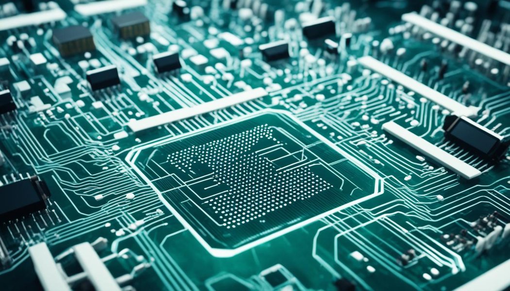
AI and VLSI integration in chip design, highlighting the role of GPU acceleration.
Other Machine Learning Paradigms
Beyond DRL and deep neural networks, various other machine learning techniques contribute to VLSI placement optimization:
- Genetic Algorithms and Evolutionary Learning: These optimization algorithms mimic natural selection to explore the design space and find optimal or near-optimal solutions for placement, especially effective in complex, multi-objective scenarios.
- Supervised Learning: Can be used to train models on historical design data to predict optimal placement configurations or to classify design hotspots that need attention.
- Unsupervised Learning: Useful for identifying patterns and clustering similar components for more efficient placement, or detecting anomalies in design data.
Impact and Benefits of AI in VLSI Placement
The integration of AI in VLSI placement brings a multitude of benefits, transforming the landscape of semiconductor design.
Enhanced Power, Performance, and Area (PPA) Optimization
AI algorithms can analyze vast amounts of design data and identify intricate relationships that are often overlooked by human designers or traditional heuristics. This leads to superior PPA outcomes:
- Reduced Area: By optimizing cell placement and macro arrangement, AI can minimize the overall chip area, leading to more compact and cost-effective designs.
- Improved Performance: Optimized placement directly translates to shorter wirelengths and reduced signal delays, enhancing the circuit's operating speed and overall performance.
- Lower Power Consumption: AI can identify power-hungry components and suggest optimized placements and power management techniques (like voltage scaling or power gating) to reduce energy consumption.
- Better Manufacturability: By considering factors like congestion and design rule violations, AI-driven placement leads to designs that are easier and more reliable to manufacture, improving yield.
Accelerated Design Cycles and Reduced Turnaround Time
One of the most significant impacts of AI is the acceleration of the design cycle. AI automates critical tasks that traditionally require extensive manual intervention or iterative trial-and-error:
- Automated Floorplanning and Placement: AI algorithms can quickly propose and evaluate optimal chip layouts, reducing the time spent on these labor-intensive stages.
- Predictive Analysis: By predicting potential issues early in the design phase, AI reduces the need for costly redesigns and iterations.
- "One-Pass" Design Flows: Learning-based predictors can anticipate downstream outcomes, allowing for more adaptive design flows with fewer iterations, sometimes even achieving a "one-pass" design.
Overcoming Design Complexity
As semiconductor technology scales, the complexity of VLSI designs rapidly increases. AI provides the necessary tools to manage this complexity:
- Exploration of Vast Design Space: AI techniques efficiently explore the enormous design space, identifying optimal configurations that would be impossible to discover through traditional methods.
- Handling Process Variations: At nanoscale geometries, process variations introduce unpredictable behavior. AI can develop robust statistical models and adaptive design techniques to mitigate their impact.
- Generalization Across Designs: Unlike heuristics, AI models can learn to generalize from various design examples, making them more adaptable to different architectures and technology nodes.
Comparative Analysis of AI Techniques for VLSI Placement
To further illustrate the strengths of various AI techniques in VLSI placement optimization, the following radar chart provides a comparative overview. These scores are based on their typical effectiveness, development complexity, and integration potential within current EDA flows.
This radar chart visually compares the strengths of Deep Reinforcement Learning (DRL), Deep Neural Networks (DNNs), and Evolutionary Algorithms (EAs) in VLSI placement. DRL excels in overall PPA optimization and handling complexity due to its ability to learn sequential decision-making. DNNs are strong in design time reduction through predictive modeling. Evolutionary Algorithms, while robust, generally exhibit lower scores in areas like computational intensity and generalizability compared to deep learning methods, highlighting why DRL and DNNs are at the forefront of advanced AI techniques for this domain.
The Future Outlook: AI and VLSI Synergies
The synergy between AI and VLSI design is expected to deepen, leading to even more sophisticated and automated design workflows. Conferences like GLSVLSI 2025 and ISVLSI 2025 continue to showcase cutting-edge research in this area, emphasizing AI's growing role.
Beyond Placement: AI's Broad Impact on VLSI Design
While this discussion focuses on placement, AI's influence extends across the entire VLSI design flow:
| VLSI Design Stage | AI Application | Benefits |
|---|---|---|
| Floorplanning | AI algorithms propose optimized block layouts considering wirelength, congestion, and power distribution. | Intelligent arrangement of major blocks, improving initial design quality. |
| Placement | Deep Reinforcement Learning, Neural Networks for cell and macro placement optimization. | Significant PPA improvements, reduced design time, automation of complex tasks. |
| Routing | AI-driven global and detailed routing to minimize wirelength and congestion, ensure signal integrity. | More efficient and accurate routing paths, reduced iterations. |
| Timing Optimization | Predictive models to estimate performance, identify critical paths, and suggest optimizations. | Achieving timing closure faster, reducing timing violations. |
| Power Optimization | Analyzing power consumption patterns, identifying hot spots, suggesting power management techniques (voltage/clock gating). | Reduced energy consumption, extended battery life, improved thermal management. |
| Verification and Testing | Automated test pattern generation (ATPG), fault detection and diagnosis, predictive modeling for design flaws. | Improved test coverage, faster fault identification, enhanced reliability. |
| Analog Design | AI-assisted optimization of transistor sizes and circuit parameters for analog circuits. | Faster analog circuit design, especially critical for lower technology nodes. |
| Design Space Exploration | AI techniques (genetic algorithms, evolutionary algorithms, RL) to explore vast design parameters. | Identification of optimal design points, superior chip architectures. |
Challenges and Opportunities
Despite the immense potential, challenges remain. The need for vast, high-quality datasets for training, the interpretability of complex AI models, and the integration of AI tools seamlessly into existing EDA flows are ongoing areas of research and development. However, the continuous advancements in AI algorithms, coupled with increasing computational power, promise to unlock even greater efficiencies and innovations in VLSI design.
This video provides an excellent overview of how AI and VLSI work together, discussing the future outlook and potential career implications of this powerful convergence.
A discussion on the symbiotic relationship between AI and VLSI, and its impact on the future of chip design jobs.
Frequently Asked Questions (FAQ)
Conclusion
The integration of advanced AI techniques, particularly Deep Reinforcement Learning and Neural Networks, is fundamentally transforming VLSI placement optimization. These intelligent approaches enable engineers to overcome the formidable challenges posed by increasing chip complexity, leading to unprecedented levels of automation and optimization. By leveraging AI, the semiconductor industry can achieve superior Power, Performance, and Area (PPA) metrics, significantly accelerate design cycles, and explore vast design spaces that were previously intractable. As AI continues to evolve, its symbiotic relationship with VLSI design will undoubtedly drive the next wave of innovation in microelectronics, paving the way for more powerful, efficient, and cost-effective integrated circuits.
Recommended Further Exploration
- How are AI and machine learning integrated across the entire VLSI design flow, beyond just placement?
- What are the emerging trends in VLSI physical design driven by AI and automation, and what challenges do they present?
- Can you provide specific case studies or examples of commercial EDA tools leveraging AI for VLSI optimization?
- What deep learning architectures are most effective for generating optimal chip layouts and how do they compare?