
Comprehensive Guide to Dry Etching of Silicon Oxynitride (SiON)
Precision Techniques in Semiconductor Manufacturing
Key Takeaways
- Advanced Techniques: Reactive Ion Etching (RIE) and Inductively Coupled Plasma (ICP) are pivotal for achieving anisotropic etching profiles.
- Critical Parameters: Gas chemistry, plasma power, pressure, and substrate temperature must be meticulously controlled to ensure high selectivity and uniformity.
- Challenges and Solutions: Addressing issues like mask erosion, residue formation, and uniformity requires optimized gas mixtures and advanced process controls.
Introduction to Dry Etching of SiON
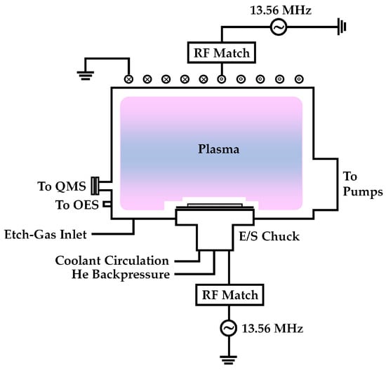
Dry etching of Silicon Oxynitride (SiON) is a fundamental process in the fabrication of advanced semiconductor devices, photonic components, and microelectromechanical systems (MEMS). SiON, a versatile dielectric material combining the properties of silicon dioxide (SiO₂) and silicon nitride (Si₃N₄), offers excellent optical characteristics, high etch resistance, and adjustable refractive indices. Dry etching techniques, particularly Reactive Ion Etching (RIE) and Inductively Coupled Plasma (ICP) etching, are preferred over wet etching due to their precision, anisotropic profiles, and compatibility with modern microfabrication processes.
Techniques Used for SiON Dry Etching
1. Reactive Ion Etching (RIE)
RIE combines both chemical reactions and physical sputtering to achieve anisotropic etching profiles. This technique is highly effective for etching SiON due to its ability to provide vertical sidewalls essential for applications like optical waveguides and MEMS structures.
- Gas Mixtures: Commonly employs fluorine-based gases such as CF₄, CHF₃, SF₆, and C₄F₈, often mixed with oxygen (O₂) to enhance etch rates and selectivity.
- Anisotropy: Ion bombardment during RIE leads to directional etching, minimizing lateral material removal and ensuring precise feature dimensions.
- Applications: Ideal for creating high aspect ratio structures in integrated circuits and photonic devices.
2. Inductively Coupled Plasma (ICP) Etching
ICP etching utilizes a high-density plasma to achieve faster etch rates and better uniformity across larger substrates compared to traditional RIE. This method provides superior control over etching parameters, making it suitable for advanced semiconductor manufacturing.
- Plasma Density: The high-density plasma generated in ICP allows for more efficient material removal and improved etch uniformity.
- Process Control: Enhanced control over etch profiles and selectivity through precise adjustment of process parameters.
- Applications: Widely used in the fabrication of silicon-based interlayer dielectrics and photonic devices requiring uniform etching across large wafers.
Mechanisms of SiON Dry Etching
1. Chemical Reactions
The dry etching process primarily relies on chemical reactions between reactive fluorine-based species and the SiON material. These reactions form volatile byproducts, such as SiF₄, CO, CO₂, and NO, which are subsequently removed from the etch chamber.
- Fluorine-Based Gases: Gases like CF₄ and CHF₃ provide fluorine radicals that react with silicon, oxygen, and nitrogen in SiON.
- Volatile Byproducts: The formation of volatile compounds ensures efficient material removal and prevents the redeposition of etched materials.
2. Ion Bombardment
In addition to chemical reactions, physical sputtering caused by ion bombardment contributes to the etching process. This mechanism breaks bonds within the SiON layer, enhancing the overall etch rate and contributing to the anisotropy of the etch profile.
- Ion Energy: Controlled ion energy is critical to balance between effective etching and minimizing substrate damage.
- Anisotropic Etching: Directed ion bombardment ensures vertical sidewalls, which are essential for high-precision device structures.
3. Process Optimization
Optimizing the etching process involves adjusting various parameters to achieve desired selectivity and etch profiles. Key aspects include gas chemistry optimization, plasma power adjustment, pressure control, and substrate temperature management.
- Selectivity: Achieved by fine-tuning the gas mixture and plasma conditions to preferentially etch SiON over other materials like silicon or SiO₂.
- Profile Control: Ensuring vertical sidewalls and minimizing surface roughness through precise parameter adjustments.
Critical Parameters in SiON Dry Etching
1. Gas Chemistry
The choice of gases is pivotal in determining the etch rate, selectivity, and profile of the etched SiON. Fluorocarbon gases are extensively used due to their reactive properties with SiON.
| Gas | Purpose | Effects |
|---|---|---|
| CF₄ (Carbon Tetrafluoride) | Provides fluorine radicals for chemical etching | Enhances etch rate and selectivity |
| CHF₃ (Trifluoromethane) | Introduces both fluorine and carbon species | Balances etch rate with polymer formation for anisotropy |
| SF₆ (Sulfur Hexafluoride) | Supplies fluorine radicals | Increases etch rate and contributes to selectivity |
| O₂ (Oxygen) | Enhances removal of polymer residues | Improves surface cleanliness and etch precision |
| Ar (Argon) | Promotes physical sputtering | Enhances anisotropic etching by increasing ion bombardment |
2. Plasma Power
Plasma power determines the energy of ions within the plasma. Higher plasma power increases ion energy, enhancing the etch rate and anisotropy but may also lead to substrate or mask damage.
- High Plasma Power: Leads to faster etch rates and more directional etching but risks damaging sensitive materials.
- Low Plasma Power: Reduces the risk of substrate damage but may result in lower etch rates and less anisotropy.
3. Chamber Pressure
Chamber pressure influences the mean free path of ions and reactive species. Lower pressures generally promote anisotropic etching by reducing collisions, making the etch process more directional.
- Low Pressure: Enhances anisotropy and etch precision.
- High Pressure: Increases lateral etching and can lead to less defined etch profiles.
4. Substrate Temperature
While etching is typically performed at or near room temperature, substrate temperature can affect the etch rate and selectivity. Higher temperatures may increase etch rates but can also lead to unwanted thermal effects.
- Temperature Control: Essential for maintaining consistent etch rates and preventing thermal damage to materials.
- Cooling Systems: Often employed to manage substrate temperature during high-power plasma operations.
5. Bias Voltage
The bias voltage applied to the substrate controls the acceleration of ions toward the surface, affecting the etch rate and anisotropy.
- High Bias Voltage: Increases ion energy, enhancing etch rates and sidewall anisotropy.
- Low Bias Voltage: Reduces etch rates and minimizes potential damage to the substrate.
Challenges in Dry Etching of SiON
1. Selectivity to Underlying Layers
Achieving high selectivity between SiON and underlying materials such as silicon, SiO₂, or Indium Tin Oxide (ITO) is crucial. Low selectivity can result in unintended etching of these layers, compromising device integrity.
- Optimization: Fine-tuning gas chemistry and plasma parameters can enhance selectivity.
- Etch-Stop Layers: Incorporating materials like Al₂O₃ as thin etch-stop layers can protect underlying structures during SiON etching.
2. Residue Formation
Polymer residues can form during the etching process, leading to surface contamination and requiring additional cleaning steps, which can introduce defects.
- Mitigation: Adding oxygen to the gas mixture helps in reducing polymer formation, ensuring cleaner etch profiles.
- Post-Etch Cleaning: Implementing effective cleaning protocols post-etching to remove any residual polymers.
3. Mask Erosion
The integrity of the photoresist mask is vital for maintaining accurate etch patterns. Mask erosion can occur due to intense plasma exposure, especially during deep etching processes.
- Resilient Mask Materials: Utilizing mask materials with higher resistance to plasma erosion.
- Protective Coatings: Applying protective coatings or using passivation steps to extend mask longevity.
4. Etch Uniformity
Uniform etching across large wafers poses a significant challenge, as variations can lead to inconsistencies in device performance.
- Plasma Distribution Control: Balancing the plasma distribution through meticulous adjustment of process pressure, RF power coupling, and gas flow dynamics.
- Equipment Calibration: Regular calibration and maintenance of etching equipment to ensure consistent performance.
Applications of SiON Dry Etching
1. Integrated Photonic Devices
SiON dry etching is essential in crafting optical waveguides, where precise control over etch depth and sidewall profiles ensures effective light propagation and minimal loss.
- Waveguides: High aspect ratio grooves for guiding light in photonic circuits.
- Modulators and Switches: Fabrication of active components requiring fine etch precision.
2. Semiconductor Interlayer Dielectrics
In advanced semiconductor stacks, SiON serves as a reliable insulating layer. Dry etching ensures that these layers are accurately patterned without affecting adjacent materials.
- Insulation: Prevents electrical interference between different device layers.
- Capacitance Control: Precise etching contributes to accurate capacitance values in integrated circuits.
3. MEMS Devices
Microelectromechanical Systems (MEMS) rely on dry-etched SiON layers to form intricate, high aspect ratio structures necessary for sensors and actuators.
- Pressure Sensors: Etched SiON cavities for detecting minute pressure changes.
- Optical MEMS: Structures that manipulate light within MEMS-based optical devices.
Advancements in SiON Etching
1. Cyclic Etching Techniques
Innovative cyclic etching methods, akin to Bosch processes used in deep silicon etching, involve alternating etch and passivation steps. This approach enhances vertical sidewall profiles and reduces lagging effects.
- Vertical Profiles: Achieves near-vertical sidewalls essential for high-precision applications.
- Reduced Lagging: Minimizes the formation of undercuts and ensure uniform etching.
2. Integration of Machine Learning
Machine learning algorithms are being employed to optimize etching parameters dynamically, leading to higher yields and more consistent manufacturing outcomes.
- Parameter Optimization: Real-time adjustments based on predictive models to maintain optimal etch conditions.
- Process Control: Enhanced monitoring and control mechanisms to detect and correct deviations promptly.
3. Advanced Chemical Controls
Developments in chemical formulations and process controls are contributing to reduced contamination levels and enhanced selectivity during multi-layer etching processes.
- Enhanced Selectivity: Improved chemistries allow for selective etching of SiON without compromising adjacent layers.
- Contamination Reduction: Advanced process controls minimize unwanted chemical interactions and deposition.
Advantages of Dry Etching Over Wet Etching
Dry etching offers numerous benefits compared to traditional wet etching methods, making it the preferred choice in modern semiconductor fabrication.
-
Precision: Superior control over etch depth and profile, enabling high-resolution patterning.
-
Anisotropy: Minimal lateral etching ensures well-defined vertical sidewalls.
-
Compatibility: Better integration with advanced microfabrication processes and materials.
-
Reduced Waste: Generates fewer chemical byproducts, aligning with environmentally friendly manufacturing practices.
-
Reproducibility: More consistent etching results across multiple wafers and batches.
Conclusion
The dry etching of Silicon Oxynitride (SiON) stands as a cornerstone in the realm of semiconductor and photonic device fabrication. Employing advanced techniques like Reactive Ion Etching (RIE) and Inductively Coupled Plasma (ICP) etching allows for precise, anisotropic etching profiles essential for high-performance applications. Mastery over critical parameters such as gas chemistry, plasma power, and chamber pressure is paramount to achieving high selectivity and uniformity. Despite challenges like mask erosion and residue formation, ongoing advancements in cyclic etching techniques and the integration of machine learning are paving the way for more efficient and reliable etching processes. As the semiconductor industry continues to evolve, the role of dry etching in shaping the intricate architectures of future devices remains indispensable.
References
Last updated January 21, 2025