
Analyzing Electrostatic Effects on Capacitive Sensor Performance
Understanding challenges and developing solutions for touch-based systems
Highlights
- Electrostatic Interference and Sensitivity Loss - Electrostatic interference can cause false triggering and measurement errors, leading to reduced sensitivity and reliability in sensor data.
- Environmental and Material Influences - Factors such as humidity, temperature, and material properties can affect the accumulation and distribution of charges, impacting overall sensor performance.
- Design and Compensation Strategies - Optimizing sensor design and implementing compensation methods are crucial for mitigating the adverse effects of electrostatic charges.
Introduction
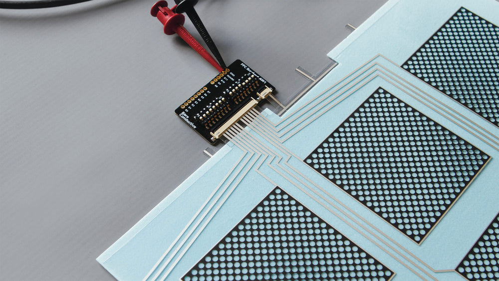
In touch-based systems, the performance of capacitive sensors is critical to user experience and device functionality. Capacitive sensors operate based on the measurement of capacitance changes when a conductive object, such as a human finger, interacts with the sensor surface. However, the presence of electrostatic charges in the environment or generated through human interaction can introduce significant challenges. These challenges disrupt the sensor's accuracy and reliability, manifesting through false triggers, sensitivity loss, and other measurement inconsistencies.
Electrostatic charges can arise from various sources including triboelectric effects, environmental conditions like high humidity, and variations in temperature. Moreover, the design of sensor systems—including layout, material selection, and shielding techniques—plays an essential role in defining how well a sensor system resists or compensates for these undesired effects. Developing precise problem statements is necessary to systematically address these challenges, paving the way for improved sensor accuracy and performance in real-world applications.
Detailed Analysis of the Problem Statements
Creating specific problem statements is a crucial step in addressing the issues induced by electrostatic charges in capacitive sensing. The following sections articulate several problem statements that collectively cover the spectrum of challenges that engineers and researchers might encounter.
1. Electrostatic Field Interference
Statement: "How do environmental electrostatic fields impact the sensitivity and accuracy of capacitive touch sensors in high-interference conditions?"
Key Considerations
- The presence of ambient electrostatic fields can distort the electric field generated by the sensor, resulting in false or inaccurate readings.
- Variations in the external electromagnetic environment, such as those found in industrial settings or areas with significant electronic noise, can exacerbate sensor inaccuracies.
- Research must focus on quantifying measurement uncertainties and developing techniques to shield or adapt sensor responsiveness under varying field strengths.
2. Parasitic Capacitance and Signal Distortion
Statement: "To what extent does parasitic capacitance arising from nearby conductive elements contribute to signal distortion and measurement errors in capacitive sensing systems?"
Key Considerations
- Unintended capacitive couplings, particularly those resulting from grounded planes and surrounding conductive materials, introduce parasitic effects.
- This additional, unwanted capacitance influences the sensor’s net capacitance value, thereby affecting accuracy.
- Strategies are required to isolate the active sensing electrode from such parasitic influences through effective layout design and shielding techniques.
3. Human Body Electrostatic Interaction
Statement: "How do the inherent electrostatic properties of the human body affect the performance of capacitive touch sensors during routine interactions?"
Key Considerations
- Human interaction introduces variability in sensor measurements due to differences in skin conductivity, moisture levels, and inherent static charges.
- Each user interaction can result in varied capacitance values, necessitating adaptive calibration and compensation algorithms.
- Understanding the charge transfer mechanisms at the interface between human skin and the sensor surface is essential for mitigating false positives and improving detection consistency.
4. Impact of Humidity and Temperature
Statement: "What are the effects of ambient humidity and temperature fluctuations on the distribution of electrostatic charges on sensor surfaces, and how do these changes alter sensor performance over time?"
Key Considerations
- Environmental variables such as humidity and temperature have a significant impact on the behavior of electrostatic charges; they can lead to charge accumulation or dispersion on sensor surfaces.
- These changes can result in a drift in sensor response, leading to inconsistencies in touch detection.
- Developing temperature compensation and humidity-resistant sensor designs is a key area for research to ensure consistent performance in diverse environments.
5. Electrostatic Discharge (ESD) Effects
Statement: "How do episodes of electrostatic discharge (ESD) impact the structural integrity and operational longevity of capacitive touch sensors, and what mitigation strategies can enhance system resilience?"
Key Considerations
- ESD events introduce sudden surges in static charge that can disrupt sensor functionality or even cause physical damage to sensitive components.
- Investigating the transient behavior of sensors during ESD events helps in understanding the recovery and resilience of these systems.
- Adopting materials with higher ESD tolerance and incorporating protective circuit elements can significantly improve the overall durability and reliability of touch screens.
6. Design Optimization for Electrostatic Mitigation
Statement: "Which design modifications and material choices can effectively mitigate the adverse effects of accumulated electrostatic charges on capacitive sensor performance, and how can these improvements be quantified?"
Key Considerations
- Sensor design plays a pivotal role in managing electrostatic interference; factors such as electrode geometry, material selection, and sensor layout contribute to performance.
- Exploration of alternative materials and sensor configurations offers pathways to reduce the impact of parasitic and uncontrolled capacitance.
- Quantitative metrics such as signal-to-noise ratio (SNR) and capacitance drift are vital in evaluating the efficacy of different design optimizations.
Comparative Overview of Problem Statements
To better synthesize the variety of identified issues, the following table presents an overview that highlights the unique challenges and focal points within each problem statement:
| Problem Statement | Key Considerations | Research Focus |
|---|---|---|
| Electrostatic Field Interference | Environmental charge distortion, measurement uncertainties | Quantitative shielding and field compensation |
| Parasitic Capacitance and Signal Distortion | Unwanted capacitive coupling, layout-induced errors | Mitigation through design improvements and isolation techniques |
| Human Body Electrostatic Interaction | User variability in charge transfer, skin conductivity | Adaptive calibration and algorithm development |
| Impact of Humidity and Temperature | Environmental factors influencing charge accumulation | Temperature and humidity compensation strategies |
| Electrostatic Discharge (ESD) Effects | Transient high-charge impacts, component degradation | Resilience design and improved ESD protection |
| Design Optimization for Electrostatic Mitigation | Material properties, electrode geometry | Performance quantification through enhanced design and measurement techniques |
In-Depth Discussion
Electrostatic Interference and Sensitivity Loss
One of the primary challenges encountered in capacitive touch systems is the interference caused by ambient electrostatic fields. These fields can introduce unexpected changes in capacitance by distorting the electric field around the sensor, which is especially detrimental in areas with high electronic activity. Even small variations in the ambient static field can cause the sensor to register phantom touches or miss intended interactions, leading to a diminished user experience. In addition, variations in the field can create offset errors in the sensor output, hence undermining the device's reliability.
Mitigating these effects requires a dual approach: the adoption of advanced shielding methods to contain unwanted electrostatic fields and the implementation of robust sensor algorithms that can adaptively adjust to the fluctuating baseline conditions. Researchers continue to explore the potential of improved PCB (Printed Circuit Board) layout techniques and grounding strategies to minimize the influence of ambient disturbances.
Influence of Material Properties and Environmental Factors
The performance of capacitive sensors is not solely governed by external fields but also by the inherent properties of the materials used in their construction. The selection of sensor materials, including the electrodes and the dielectric layers, directly affects how charges accumulate and dissipate on the sensor surface. Environmental factors—specifically humidity and temperature—play a significant role in influencing these material properties. For example, high humidity conditions may facilitate charge accumulation through enhanced ionic conduction, while temperature variations can lead to changes in the capacitance of materials.
Optimizing sensor performance under variable conditions necessitates comprehensive environmental testing combined with the development of compensation techniques. Establishing a clear understanding of these dependencies allows for the creation of sensors that maintain stability even as temperature and humidity fluctuate.
Strategies for Improved Sensor Design
Addressing the adverse impacts of electrostatic charges requires rethinking sensor design. By reconfiguring the electrode geometry, improving material selection, and introducing enhanced shielding techniques, engineers can reduce unintended capacitance contributions and improve overall sensor accuracy. A notable focus is on reducing parasitic capacitance—often an overlooked aspect that compromises the reliability of the sensor system.
The application of advanced compensation algorithms is also at the forefront of research. These algorithms adjust the sensor's output by dynamically compensating for baseline drifts and other offsets introduced by variable electrostatic conditions. Such strategies are pivotal in maintaining calibrated sensor states, particularly in consumer electronics like smartphones and tablets, where device orientation and user handling can further influence static charge distribution.
Challenges Arising from Electrostatic Discharge (ESD)
Electrostatic Discharge (ESD) events represent another critical challenge in the performance of capacitive sensors. ESD can induce rapid and often destructive surges of static energy, leading to short-term sensor malfunctions or permanent damage. The delicate components in modern touch interfaces are particularly vulnerable to these high-energy incidents.
Research into ESD mitigation focuses on both materials engineering and circuit design. The incorporation of protective circuit elements, as well as leveraging materials with superior discharge tolerance, can significantly enhance the resilience of the overall system. Understanding the transient behavior of sensors during ESD also informs the development of recovery protocols that minimize downtime and maintain operational integrity.
Integrative Design Optimization
A holistic approach to mitigating the adverse effects of electrostatic charges involves the integrative optimization of sensor design. This begins with a careful analysis of the sensor’s immediate electrical environment, including considerations for surrounding conductive surfaces and layout topologies. By integrating the insights derived from examining environmental factors, parasitic capacitance, and dynamic human interactions, engineers can propose design modifications that inherently resist or nullify the detrimental effects of static charge build-up.
In practice, optimizing the design may involve innovations in PCB technology, such as multilayer board designs that incorporate dedicated ground planes and electromagnetic shielding layers. Additionally, exploring new dielectric materials with more stable electrical properties under varying environmental conditions can further reduce inconsistencies in sensor outputs. These design improvements are crucial in industrial applications where reliability and long-term operational consistency are paramount.
References
-
Electrostatic forces and their effects on capacitive mechanical sensors - ScienceDirect
- Capacitive sensing - Wikipedia
- Electrostatic Sensors – Their Principles and Applications - Kent University
- Understanding Electrostatic Discharge (ESD) in Touchscreen Technology - TouchPro
- Recent Advances of Capacitive Sensors: Materials and Microstructures - Wiley Online Library
- Effects of Electrostatic Forces on Capacitive Sensors - Harvard ADS
- Comparison of Sensor Technologies - Automation Primer
-
Electrostatic sensors: Their principles and applications - ScienceDirect
- Advanced Capacitive Sensor Designs - Wiley
- Capacitive Touchscreen Durability in ESD Conditions - TouchPro
Recommended Related Queries
Last updated March 3, 2025