
From Pixels to Powerhouses: The Unstoppable Evolution of the GPU
Charting the incredible journey of Graphics Processing Units, from gaming origins to AI dominance and beyond.
Key Highlights
- From Niche to Necessity: GPUs evolved from specialized 2D/3D graphics hardware in the 90s into indispensable parallel processors driving AI, scientific computing, and data analytics today.
- Manufacturing Marvels: Modern GPUs are feats of engineering, fabricated using cutting-edge nanometer technology by giants like TSMC and Samsung, involving intricate design, assembly, and testing.
- Innovation & Challenges: Key breakthroughs like programmable shaders, CUDA, and AI-specific cores propelled GPU capabilities, while challenges like power consumption, heat dissipation, and supply chain logistics persist.
In the dynamic realm of computing technology, few components have undergone such a dramatic and impactful transformation as the Graphics Processing Unit (GPU). Initially conceived to render the increasingly complex visuals of video games and specialized design applications, the GPU has evolved far beyond its graphical origins. Today, it stands as a cornerstone of modern computing, a massively parallel processing engine essential for artificial intelligence, high-performance computing, scientific discovery, and countless other data-intensive tasks. This article delves into the rich history of the GPU, tracing its evolution from early graphics adapters to the sophisticated silicon powering our digital world, exploring the intricate manufacturing processes, pivotal innovations, current capabilities, and the hurdles overcome along its remarkable journey.
The Genesis: Planting the Seeds for Visual Computing
Early Graphics and the Quest for 3D
The roots of the GPU can be traced back to the 1970s and early 1980s, long before the term "GPU" existed. Early computer systems relied on basic video adapters like IBM's Monochrome Display Adapter (MDA) and Color Graphics Adapter (CGA) to handle rudimentary 2D output – primarily text and simple shapes. These early cards laid the groundwork, but the demand for more sophisticated visuals grew, particularly from industries like computer-aided design (CAD) for automotive and aerospace engineering, military simulations, and medical imaging.
The real catalyst for modern GPU development arrived in the mid-1990s. The convergence of more affordable personal computers, the adoption of 32-bit operating systems, and the burgeoning video game market created a fervent demand for realistic 3D graphics. 1995 saw the introduction of the first dedicated 3D add-in graphics cards, marking a significant leap. Companies like 3dfx Interactive (with its Voodoo series), ATI Technologies (later acquired by AMD), and NVIDIA entered a period of intense competition and innovation, often referred to as the "wild west" of graphics hardware.
The Birth of the "GPU": NVIDIA's GeForce 256
A pivotal moment occurred in 1999 when NVIDIA launched the GeForce 256. More than just a powerful graphics card, NVIDIA boldly marketed it as the "world's first GPU." This distinction wasn't merely marketing hype; the GeForce 256 integrated hardware-based transform and lighting (T&L) capabilities directly onto the chip. Previously, these computationally intensive 3D calculations were handled by the CPU. Offloading T&L to the graphics card freed up the CPU and significantly accelerated 3D rendering performance, setting a new standard for graphics architecture.
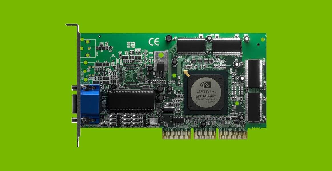
The NVIDIA GeForce 256, marketed as the world's first GPU, introduced integrated Transform & Lighting in 1999.
Evolution Through Innovation: Unleashing Parallel Power
From Fixed Functions to Programmability
Early GPUs operated on a "fixed-function pipeline." This meant the hardware was designed to perform specific, predefined graphics tasks (like T&L or pixel shading) in a rigid sequence. While efficient for contemporary games, this approach lacked flexibility.
The early 2000s ushered in the era of programmability. Graphics cards like ATI's Radeon 8500 and NVIDIA's GeForce 3 (released in 2001) introduced programmable shaders. This revolutionary step allowed developers to write custom programs (shaders) that could run directly on the GPU, enabling much more sophisticated and dynamic visual effects, such as realistic lighting, shadows, and material properties. This programmability laid the crucial groundwork for using GPUs beyond mere graphics rendering.
GPGPU: The Parallel Processing Revolution
Recognizing the immense parallel processing potential inherent in GPU architecture (designed to handle thousands of pixels simultaneously), researchers and engineers began exploring ways to harness this power for non-graphical tasks. This concept became known as General-Purpose computing on Graphics Processing Units (GPGPU).
A major breakthrough arrived in 2007 with NVIDIA's introduction of CUDA (Compute Unified Device Architecture). CUDA provided a software platform and programming model that made it significantly easier for developers to write code that could execute complex parallel computations on NVIDIA GPUs. This opened the floodgates for GPUs to be used in scientific research, financial modeling, data analysis, and other computationally intensive fields. Two years later, the cross-platform OpenCL (Open Computing Language) framework emerged, offering a more portable alternative for programming diverse parallel processors, including GPUs and CPUs from different vendors.
This shift transformed the GPU from a graphics-specific accelerator into a powerful, programmable parallel processor, fundamentally altering the landscape of high-performance computing.
Inside the Silicon Forge: The Art of GPU Manufacturing
Creating a modern GPU is an incredibly complex process, pushing the boundaries of physics and engineering. It involves meticulous design, advanced materials science, and ultra-precise manufacturing techniques carried out in highly specialized facilities.
Phase 1: Design and Architecture
The journey begins long before any silicon is etched. Teams of engineers at companies like NVIDIA and AMD design the GPU's architecture. This involves:
- High-Level Design: Defining the overall structure, features, performance targets, and power budget.
- Logic Design (RTL): Writing detailed descriptions of the chip's functionality using hardware description languages (HDLs).
- Physical Design: Creating the intricate physical layout, mapping out the placement of billions of transistors and the complex web of interconnects (the "floorplan" and "netlist").
- Verification & Emulation: Running extensive simulations and emulations on powerful computer systems to verify the design's correctness and predict its performance before committing to costly manufacturing.
Phase 2: Fabrication (The Foundry)
Once the design is finalized, it's sent to a semiconductor foundry – a highly specialized factory equipped for chip manufacturing. Leading foundries like Taiwan Semiconductor Manufacturing Company (TSMC), Samsung (South Korea), and SK Hynix (South Korea) handle the fabrication for major GPU designers.
The Nanoscale Process
The core process involves photolithography on large silicon wafers:
- Wafer Preparation: Starting with ultra-pure silicon wafers, typically 300mm in diameter.
- Layering: Applying multiple layers of different materials (conducting, insulating, semiconducting) onto the wafer.
- Photolithography: Using masks (stencils based on the chip design) and ultraviolet (UV) light (often extreme ultraviolet, or EUV, for the most advanced processes) to project the circuit patterns onto a light-sensitive chemical layer (photoresist).
- Etching: Removing exposed or unexposed material to create the transistor structures and interconnects defined by the mask pattern.
- Doping: Introducing impurities into specific areas of the silicon to alter its electrical properties, forming the transistors.
This cycle of layering, lithography, etching, and doping is repeated dozens, sometimes hundreds, of times to build up the complex, multi-layered structure of the GPU chip. Manufacturing occurs in "cleanrooms" – environments thousands of times cleaner than a hospital operating room – to prevent microscopic dust particles from causing defects. The scale is staggering: modern GPUs contain billions of transistors packed into a few square centimeters, with features measured in nanometers (billionths of a meter). For instance, Samsung has produced NVIDIA GPUs using 3-nanometer technology.
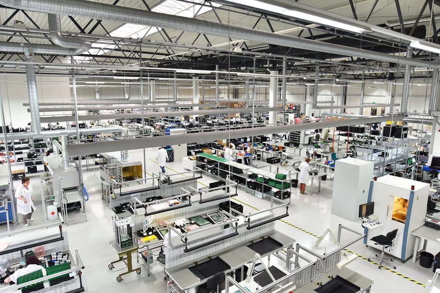
Inside a semiconductor fabrication facility (cleanroom) where GPU chips are manufactured.
Phase 3: Assembly, Testing, and Packaging
From Wafer to Chip
After fabrication, the individual chips (called "dies") on the wafer are tested for defects. The wafer is then precisely cut (diced) to separate the individual dies.
Building the Graphics Card
Functional dies are then sent to assembly facilities. Here, the GPU die is mounted onto a substrate and then onto the main Printed Circuit Board (PCB). Other critical components are added:
- Video Memory (VRAM): High-speed memory chips (like GDDR6X) that store textures and other data the GPU needs quick access to.
- Power Delivery System: Voltage regulator modules (VRMs) and capacitors to provide stable power.
- Cooling Solution: Heatsinks (often copper/aluminum fins), heat pipes, fans, or even liquid cooling blocks to dissipate the significant heat generated.
- Connectors: Display outputs (HDMI, DisplayPort), power connectors, and the interface connector (typically PCIe) for the motherboard.
Assembly often involves highly automated processes, with machines placing tiny surface-mount components onto the PCB, followed by soldering. Human oversight remains crucial for quality control.
Rigorous Testing
Completed graphics cards undergo extensive testing, including performance benchmarks, thermal stress tests, signal integrity checks, and even acoustic tests to measure noise levels from fans, sometimes requiring environments with background noise as low as 12-13dB.
Finally, the cards are packaged with drivers, manuals, and accessories, ready for shipment to distributors and consumers.
Mapping the GPU Journey
The evolution of GPUs involves distinct phases of technological advancement and shifts in manufacturing focus. This mindmap outlines the key stages from early graphics processing to modern parallel computing powerhouses and the intricate production process.
'First GPU'
Hardware T&L"] id2["Key Innovations"] id2a["Programmable Shaders (Early 2000s)"] id2b["GPGPU Emergence"] id2b1["NVIDIA CUDA (2007)"] id2b2["OpenCL (2009)"] id2c["Massive Parallelism"] id2d["AI Acceleration (Tensor Cores)"] id2e["Real-Time Ray Tracing (RT Cores)"] id2f["Chiplet Architectures"] id3["Manufacturing Process"] id3a["Design Phase"] id3a1["Architecture Blueprint"] id3a2["Logic & Physical Design"] id3a3["Verification & Emulation"] id3b["Fabrication (Foundries: TSMC, Samsung)"] id3b1["Silicon Wafers"] id3b2["Photolithography (nm scale, EUV)"] id3b3["Layering, Etching, Doping"] id3b4["Cleanroom Environment"] id3c["Assembly & Testing"] id3c1["Wafer Dicing & Die Testing"] id3c2["PCB Mounting (GPU, VRAM, VRM)"] id3c3["Cooling Solution Integration"] id3c4["Performance & Stress Testing"] id4["Modern Applications"] id4a["Gaming (High Fidelity, VR)"] id4b["Artificial Intelligence & Machine Learning"] id4c["High-Performance Computing (HPC)"] id4d["Data Centers & Cloud Computing"] id4e["Professional Visualization"] id4f["Cryptocurrency Mining (Historically)"] id5["Challenges"] id5a["Manufacturing Complexity & Cost"] id5b["Power Consumption & Heat"] id5c["Supply Chain Vulnerability"] id5d["Limits of Moore's Law"] id5e["Software & API Ecosystem"] id5f["Environmental Impact"]
Charting GPU Advancement Across Eras
The evolution of GPUs can be visualized by tracking key characteristics across different technological eras. This radar chart provides an estimated representation of how aspects like performance, parallelism, programmability, application scope, and manufacturing complexity have changed, highlighting the trade-offs and advancements over time. Note that values are relative estimates for illustrative purposes, not precise measurements.
As the chart illustrates, while raw performance and parallelism have seen dramatic increases, the challenges associated with power efficiency and manufacturing complexity have also grown significantly, especially in the modern era dominated by AI and large-scale computing demands.
The Modern GPU: A Computing Powerhouse
Today, GPUs are vastly different beasts compared to their ancestors. They feature thousands of processing cores (often called CUDA cores by NVIDIA or Stream Processors by AMD) operating in parallel, supported by large amounts of high-bandwidth memory. Their capabilities extend far beyond rendering pixels:
- Gaming: Powering ultra-realistic graphics with technologies like real-time ray tracing for lifelike lighting and reflections, and AI-driven upscaling (like NVIDIA DLSS or AMD FSR) for higher frame rates.
- Artificial Intelligence (AI) & Machine Learning (ML): GPUs are the workhorses for training complex deep learning models due to their aptitude for matrix multiplication and parallel computation. Specialized cores (like NVIDIA's Tensor Cores) further accelerate AI tasks.
- High-Performance Computing (HPC): Used in supercomputers for scientific simulations in fields like climate modeling, drug discovery, astrophysics, and fluid dynamics.
- Data Centers & Cloud Computing: Powering cloud gaming services, virtual workstations, video transcoding, and large-scale data analytics.
- Professional Visualization: Used by designers, architects, and content creators for complex rendering, simulation, and virtual reality applications.
The market is largely dominated by NVIDIA and AMD, whose constant competition drives rapid innovation, leading to generational leaps in performance, efficiency, and features. Intel has also re-entered the discrete GPU market, adding another layer of competition.
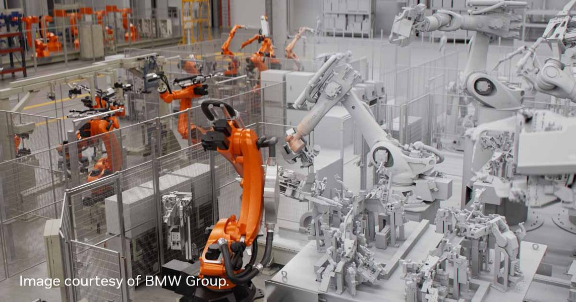
Modern GPUs are integral to AI applications across various industries, including advanced manufacturing.
Key Milestones in GPU History
The journey of the GPU is marked by significant technological advancements and product releases. This table summarizes some of the key milestones:
| Year | Milestone/Technology/GPU | Significance |
|---|---|---|
| 1995 | First 3D Add-in Cards | Beginning of dedicated 3D acceleration hardware for PCs. |
| 1999 | NVIDIA GeForce 256 | Marketed as the "first GPU"; integrated hardware Transform & Lighting (T&L). |
| 2001 | NVIDIA GeForce 3 / ATI Radeon 8500 | Introduction of programmable vertex and pixel shaders, enabling more flexible and advanced visual effects. |
| 2006-2007 | NVIDIA CUDA Launch | Provided a platform for General-Purpose GPU (GPGPU) computing, unlocking parallel processing for non-graphics tasks. |
| 2009 | OpenCL 1.0 Ratification | Established an open standard for parallel programming across heterogeneous systems (CPUs, GPUs, etc.). |
| ~2012 onwards | Rise of GPU in AI/ML | GPUs become essential for training deep neural networks due to massive parallelism. |
| 2017 | NVIDIA Volta Architecture (Tensor Cores) | Introduced specialized cores designed to accelerate AI inference and training workloads. |
| 2018 | NVIDIA Turing Architecture (RTX / RT Cores) | Brought real-time ray tracing capabilities to consumer graphics cards via dedicated RT cores. |
| 2020s | Advanced Nanometer Processes (e.g., 7nm, 5nm, 3nm) & Chiplets | Continued transistor shrinking enables greater density and performance; chiplet designs emerge to improve yield and scalability (e.g., AMD RDNA 3). |
Visualizing the GPU Timeline
For a dynamic look back at the key moments and cards that defined GPU history, particularly from the perspective of gaming and consumer hardware from 1999 onwards, the following video provides an excellent visual overview:
This video chronicles the evolution of graphics cards from the influential GeForce 256 up to modern high-end GPUs, showcasing the leaps in performance and features over two decades.
Navigating the Hurdles: Challenges in GPU Development
The path of GPU evolution has not been without significant obstacles. Developers and manufacturers have faced numerous technical, logistical, and economic challenges:
- Manufacturing Complexity & Cost: As transistors shrink to atomic scales, the cost and complexity of fabrication soar. Achieving high yield rates (the percentage of functional chips per wafer) becomes increasingly difficult, contributing to the high price of cutting-edge GPUs. Advanced lithography techniques like EUV are extraordinarily expensive.
- Power Consumption & Heat Dissipation: Packing billions of transistors running at high speeds generates immense heat. Designing effective cooling solutions (air or liquid) without excessive noise or size is a constant engineering battle. High-end GPUs now often demand powerful, dedicated power supplies (PSUs) and can significantly increase system energy consumption.
- Supply Chain Constraints: The reliance on a few specialized foundries (primarily TSMC and Samsung) makes the supply chain vulnerable to geopolitical tensions, natural disasters, and global events (as seen during the 2020-2023 chip shortages). This can lead to scarcity and price volatility.
- Physical Limits (End of Moore's Law?): While engineers continue to find ingenious ways to pack more transistors, the physical limits of silicon-based computing are approaching. Continued performance gains increasingly rely on architectural innovations, specialized accelerators (like Tensor/RT cores), and advanced packaging techniques (like chiplets) rather than just shrinking transistors.
- Software Ecosystem & API Fragmentation: Developing software that fully utilizes GPU capabilities requires specialized programming skills and tools (like CUDA or OpenCL). Competition between graphics APIs (DirectX, Vulkan, Metal) can sometimes create fragmentation for developers targeting multiple platforms.
- Environmental Concerns: The significant energy consumption of powerful GPUs, especially when deployed at scale in data centers or for tasks like cryptocurrency mining (historically), raises concerns about the environmental footprint of high-performance computing.
Despite these challenges, continuous innovation in architecture, materials science, cooling technology, and software optimization ensures that GPUs remain at the forefront of computing.
Frequently Asked Questions (FAQ)
What's the fundamental difference between a CPU and a GPU?
Who actually designs and manufactures GPUs?
What does GPGPU (General-Purpose GPU) mean?
Why are high-end GPUs so expensive and power-hungry?
Recommended Reading
- Explore how the parallel architecture of GPUs dramatically speeds up artificial intelligence model training.
- Discover the cutting-edge methods being used to manage heat in powerful modern graphics cards.
- Understand the different design philosophies and strengths of the major players in the GPU market.
- Learn more about the critical role foundries play in the semiconductor supply chain for GPUs and other technologies.
References
Last updated May 4, 2025