
Comprehensive Analysis of Intel's Fab 52
Deep dive into technology, construction, economic impact, and advanced process nodes
Key Takeaways
- Location & Scale: Fab 52 is constructed as part of a large-scale $20 billion expansion in Chandler, Arizona, integrated with other cutting-edge facilities.
- Advanced Technology: Emphasizes production using next-generation process nodes such as Intel’s 18A and 20A with innovative transistor architectures like RibbonFET.
- Economic & Employment Impact: Supports thousands of high-tech and construction jobs, as well as indirect job creation exceeding 15,000 roles within the local community.
Introduction
Intel's Fab 52 has emerged as a pivotal component in the company’s ambitious strategy to bolster its domestic semiconductor manufacturing capabilities. The facility, located at Intel's Ocotillo campus in Chandler, Arizona, is part of a broader, multi-billion-dollar expansion project aimed at ensuring the robustness and competitiveness of Intel in the evolving global semiconductor industry. This comprehensive analysis delves into various aspects of Fab 52, including its construction progress, technological innovations, production timeline, and the significant economic impact it will have on the local community. With detailed insights into advanced process nodes, facility features, and workforce contributions, this analysis provides a deep understanding of Fab 52's role in Intel’s transformation and broader industry trends.
Background & Context
Overview of Intel’s Manufacturing Strategy
Over the past decade, Intel has been reimagining its fabrication capabilities to meet the surging demand for advanced semiconductors. The company’s investment in new manufacturing facilities underscores a strategic shift towards greater domestic chip production. As global supply chain dynamics and increasing geopolitical considerations push manufacturers to localize production, Intel's expansion projects, including Fab 52, have become cornerstones of this transition. The construction of state-of-the-art fabs not only ensures the creation of high-quality chips using the latest technologies, but also reinforces Intel’s dedicated approach to reinvigorate the employment landscape in regions like Arizona.
The Strategic Importance of Fab 52
Fab 52 is not an isolated venture; it forms part of Intel's larger initiative to modernize its silicon fabrication ecosystem. With multiple fabs bearing numeric designations for internal identification and strategic planning, Fab 52 stands out as a beacon of technological progression. The facility is expected to employ the most advanced process technologies including Intel’s future nodes such as 18A and 20A, marking a significant advancement over older semiconductor processes. This evolution is aligned with the industry's need to produce ever more powerful and energy-efficient chips capable of meeting the demands of everything from modern computers and servers to mobile devices and emerging IoT applications.
Detailed Insights into Intel’s Fab 52
Location and Construction
Geographical Setting
Intel’s Fab 52 is strategically located at the Ocotillo campus in Chandler, Arizona, a city in the greater Phoenix metropolitan area. The choice of Chandler is emblematic of a larger trend of investing in U.S.-based manufacturing, mitigating supply chain vulnerabilities and reducing the reliance on overseas chip production. The use of the term "fab" reflects Intel’s internally systematic approach to numbering its facilities, aligning each new project with a specific technological and operational role.
Construction Milestones
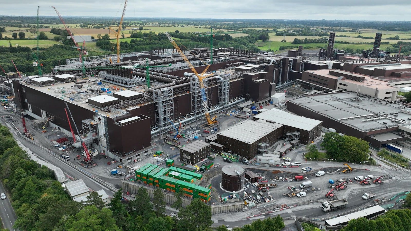
Construction of Fab 52 began in 2021 as part of a $20 billion project that also includes the twin facility Fab 62. Among the critical milestones, the recent completion of the “cheese slab” concrete pour has been a significant step; this slurry of advanced engineering forms the foundation for a multi-level facility that will eventually house over 250,000 square feet of pristine clean room space. With steel trusses already in place and the structural framework defined, the facility’s construction is both robust and emblematic of modern semiconductor cleanroom standards.
The facility's construction involves not only permanent manufacturing structures but also integrated systems to support automated production lines. The design includes specialized clean rooms with precise temperature, humidity, and particulate controls to ensure the production of defect-free wafers.
Technological Advancements and Production Capabilities
Process Nodes and Transistor Architecture
Fab 52 is designed to manufacture semiconductors using Intel’s advanced process nodes, specifically the 18A and 20A nodes. These nodes are part of Intel’s roadmap to achieving smaller, denser, and more efficient chip designs. The 18A node in particular represents a leap forward in semiconductor engineering, promising improvements in transistor performance and power efficiency.
Integral to these process nodes is the implementation of cutting-edge transistor architectures such as RibbonFET. RibbonFET technology involves innovative transistor designs that address traditional scaling challenges by offering enhanced performance and reduced power consumption. As semiconductor processes push into nanometer scales, such advancements are critical to maintaining competitive advantage.
Facility Design and Automated Production
Beyond the process nodes and transistor architectures, Fab 52 incorporates several advanced manufacturing features designed to streamline production and improve yields. One notable element is an "automated highway" integrated within the fab. This system facilitates the rapid and safe transport of materials from storage to production areas, optimizing workflow and reducing manual handling errors. In addition, the facility incorporates sophisticated automation systems to monitor and control various stages of the manufacturing process, ensuring that the wafers produced maintain the highest standards of quality.
The production lines are finely tuned for 300mm wafer lithography, which is a standard in modern semiconductor manufacture. The 300mm wafer size allows for the production of a greater number of chips per wafer compared to older 200mm standards, enhancing overall production efficiency and reducing the cost per chip.
Manufacturing Process and Cleanroom Standards
Cleanroom Architecture
The cleanroom environment is the heart of any semiconductor fabrication facility. Fab 52 boasts over 250,000 square feet of cleanroom space, meticulously designed to adhere to strict international standards. These cleanrooms maintain virtually particle-free environments crucial for preventing contamination during the photolithography and deposition stages of chip manufacturing.
This environment is achieved using an integrated system of high-efficiency particulate air (HEPA) filters, rigorous airflow designs, and environmental monitoring systems. The purpose is to create a near-sterile manufacturing zone where even microscopic contaminants are addressed immediately—a critical factor for ensuring high yields and device reliability.
Infrastructure and Utilities
Fab 52 is engineered to support a high throughput of semiconductor wafers. The facility includes multiple levels dedicated to production, air quality management, and utility support systems. Each level is designed with precision to tackle specific operational challenges. For example, the fan deck is vital for managing air flow and maintaining temperature regulations, while dedicated utility zones ensure that power, water, and other necessary inputs are continuously supplied to the cleanrooms.
Production Timeline and Future Prospects
Timeline for Production Commencement
Scheduled Production Start
Originally, Intel planned for production at Fab 52 to commence in 2024. However, evolving construction milestones and the integration of more advanced process technologies have led to some indications of delays, with the facility's production possibly starting in late 2025. Despite these potential setbacks, the strategic vision remains unchanged: once operational, Fab 52 will be at the forefront of manufacturing cutting-edge semiconductors.
The timeline for production is not merely a scheduling concern; it reflects the complexity of scaling up advanced semiconductor manufacturing. In an industry where even minor delays can have far-reaching effects on supply chains and technology development, Intel's careful pacing underscores its commitment to delivering robust, high-quality chips.
Integration with Broader Manufacturing Portfolio
Fab 52 is seamlessly integrated with Intel’s broader portfolio of fabs. Alongside its twin facility, Fab 62, the new fabs represent a massive investment aimed at enhancing overall production capacity and technological prowess. Such integration allows Intel to strategically distribute different process nodes across multiple facilities while maintaining redundancy—an essential consideration for risk management in global supply chains.
Furthermore, this integration empowers Intel to adapt to fluctuating market demands by scaling production of certain nodes over others. The facility’s flexibility enables it to switch between manufacturing priorities based on industry trends, supply shortages, or emerging technological opportunities, such as the increased need for chips in artificial intelligence applications, automotive electronics, etc.
Economic and Community Impact
Job Creation and Local Economic Boost
Direct Employment Opportunities
A significant facet of Fab 52’s development is its contribution to local and national employment. The facility is expected to create over 3,000 high-tech jobs for Intel employees, ranging from engineers and technicians to operators specializing in automated production techniques. Beyond the core workforce, construction jobs during the build phase have already amounted to nearly 3,000 positions.
These roles are not only critical to the immediate operation of the facility but also serve to foster a long-term ecosystem of technological advancement and innovation within the region. The influx of high-skilled workers often stimulates ancillary business development, including specialized services and supplier partnerships.
Indirect and Ripple Effects
The indirect impact of Fab 52 extends beyond immediate employment. Analysts estimate that the facility will generate roughly 15,000 additional jobs through its economic ripple effects. These indirect jobs come from a variety of sources, including supporting industries such as logistics, transportation, facility management, and local retail sectors.
Moreover, the presence of a state-of-the-art semiconductor facility attracts further investment into the local infrastructure—ranging from improvements in transportation networks to enhanced educational and training programs aimed at developing a skilled workforce tailored to the needs of advanced manufacturing.
Investment in Domestic Manufacturing and Long-Term Growth
Intel’s commitment to domestic manufacturing, as highlighted by its investments in Fab 52 and its sister sites, reaffirms the vital role the United States plays in the semiconductor industry. In a global market characterized by supply-chain disruptions and increasing competition, fostering a robust domestic production capacity becomes crucial.
By channeling substantial capital into new facilities, Intel not only strengthens its market position relative to global competitors but also contributes significantly to broader national goals of economic resilience and technological self-sufficiency. This strategic investment is expected to have enduring effects on innovation, research and development in semiconductor technology, and overall economic competitiveness.
Comparative Overview of Key Features
Technological and Economic Specifications
The table below provides a structured comparison of several key parameters associated with Fab 52, offering a clear snapshot of its features, capabilities, and impacts:
| Aspect | Details |
|---|---|
| Location | Ocotillo campus in Chandler, Arizona |
| Investment | Part of a $20 billion domestic expansion, with over $32 billion invested across multiple fabs |
| Process Nodes | Advanced 18A and 20A nodes featuring advanced transistor technologies such as RibbonFET |
| Cleanroom Footprint | Over 250,000 square feet of state-of-the-art, controlled environment space for production |
| Start of Production | Initially scheduled for 2024; revised expectations suggest a potential start in late 2025 |
| Job Creation | Directly over 3,000 high-tech jobs; approximately 3,000 construction jobs; 15,000 indirect jobs |
| Manufacturing Capacity | Utilizes automated production systems and advanced cleanroom technology with 300mm wafer processing capability |
Future Outlook and Industry Implications
Advancing Semiconductor Technology
The introduction of facilities like Fab 52 represents a broader paradigm shift in the semiconductor industry. With ever-decreasing node sizes and the accompanying need for higher density of transistors, the emphasis has moved towards leveraging innovations such as RibbonFET, which mitigates some of the challenges of continued scaling. Fab 52’s advanced production processes not only promise improvements in processing power and energy efficiency but also set a new standard for integrated semiconductor manufacturing. These advancements enable critical applications, ranging from data centers and cloud computing infrastructures to high-performance consumer electronics.
National and Global Impact
At a national level, the development of Fab 52 contributes significantly to the U.S. semiconductor ecosystem, bolstering domestic production capabilities. This positions the country more favorably in negotiations and competitive standpoints with international semiconductor manufacturers. Globally, stronger domestic production can lead to more stable supply chains, lower risks of disruptions and improved technological sovereignty.
Furthermore, the concentrated investments in research and development around advanced nodes in Intel's fabs encourage a competitive environment where continuous innovation becomes the norm. This ripple effect can stimulate policy reforms, incentivize further private and public investments in technology, and cultivate an ecosystem of high-tech innovation that benefits multiple sectors of the economy.
Integration with Emerging Technologies
Alongside traditional manufacturing improvements, Fab 52 is poised to play a role in supporting emergent technologies such as artificial intelligence (AI), machine learning, and next-generation high-performance computing (HPC). The cutting-edge semiconductor designs produced in this facility are critical to powering data-intensive applications and enabling breakthroughs in areas like autonomous systems and edge computing. With the evolution of these technologies, the demand for sophisticated chips that offer both power efficiency and high computational throughput is set to rise further—an area where Fab 52’s technological agenda will be instrumental.
Conclusion and Final Thoughts
Intel’s Fab 52 embodies a transformative shift in semiconductor manufacturing by setting new benchmarks in technology, production efficiency, and economic impact. From its strategic location at the Ocotillo campus in Chandler, Arizona, to its advanced process nodes and automated production lines, the facility is engineered to address current and future demands of the semiconductor market. The construction milestones, state-of-the-art cleanroom environments, and incorporation of revolutionary technologies like RibbonFET illustrate Intel’s commitment to redefining chip manufacturing standards.
Furthermore, the comprehensive job creation and economic uplift associated with Fab 52—coupled with its integration into Intel’s broader fabrication portfolio—reinforce the critical role of domestic manufacturing in sustaining technological leadership and national resilience in the semiconductor landscape. With its potential to revolutionize how chips are produced and to support emerging fields such as AI and next-generation computing, Fab 52 is not only a milestone for Intel but also a catalyst that may influence the global semiconductor industry for years to come.
References
- Two Intel Fabs Worth US $20 Billion Start Construction - Censtry
- Intel Breaks Ground on Two New Chip Factories in Arizona - Valve Magazine
- Intel Breaks Ground on Two New Leading Edge Chip Factories in Arizona - Intel
- Intel Begins Construction of Fab 52 and Fab 62 Chip Foundries in Arizona - Wccftech
- Intel Builds Arizona - Intel Newsroom
More
Last updated February 19, 2025