
Exploring ML Innovations in VLSI Design Optimization
Uncover how machine learning reshapes chip design efficiency and performance
Key Insights and Highlights
- Enhanced Design Efficiency: Machine learning (ML) accelerates design processes by automating layout generation, placement, and routing tasks.
- Improved Performance Metrics: ML-driven optimizations deliver significant improvements in power consumption, signal integrity, and overall circuit performance.
- Comprehensive Case Applications: Case studies from industry leaders and research institutions showcase real-world applications, from on-chip power grid optimization to RL-based placement for advanced processors.
Overview of ML-Driven VLSI Design Optimization
Machine learning has emerged as a transformative force in the domain of Very Large-Scale Integration (VLSI) design. By leveraging advanced algorithms and vast historical design data, designers are now able to predict, optimize, and automate various stages of the chip design lifecycle. Instead of following purely traditional methods, ML-informed techniques make use of predictive models, reinforcement learning, and genetic algorithms to tackle complex challenges in physical design automation and performance tuning. Such approaches are not just about saving time, but also about achieving significant improvements in power, performance, and area (often referred to as PPA in the semiconductor industry).
In-depth Analysis of Case Studies
1. On-Chip Power Grid Design Optimization
Efficient power distribution within a chip is critical for avoiding performance losses due to IR drop and issues arising from Electromigration. Several case studies highlight the use of ML for optimizing on-chip power grid designs.
Case Study Overview
Multiple research efforts have focused on applying supervised neural network models to predict optimal metal line widths and routing strategies. In one significant study, machine learning algorithms provided a 5-6 times speedup over traditional methods while maintaining or improving performance metrics. This approach involves training the model with extensive historical data, which captures the complex interactions of various design elements and simulated electrical performance parameters.
Benefits
- Reduced power losses and enhanced chip reliability.
- Faster turnaround times for design iterations.
- Minimized need for exhaustive manual iterations in power grid design.
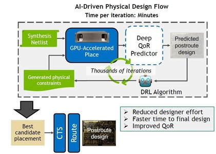
2. Physical Design Automation: Placement and Routing
Traditional physical design methods usually rely on heuristic approaches that often require significant manual intervention. ML has paved the way for automating critical tasks such as placement, floorplanning, and routing, key components of VLSI design optimization.
ML Techniques Employed
Various techniques, including reinforcement learning (RL) and genetic algorithms, have been deployed to optimize the layout of integrated circuits. A prominent example is Google’s pioneering work on using RL for the placement of Tensor Processing Units (TPUs). By intelligently rearranging macro components on a chip, these ML models are able to consistently reduce both wire lengths and delays, leading to improved timing closure (the process of ensuring signal timing constraints are met).
Benefits
- Automation of complex placement tasks reduces human error.
- Enhanced circuit performance with minimized wirelength and reduced signal delay.
- Optimized PPA outcomes, making advanced processors more efficient.
3. AI-Driven Design Space Exploration Tools
Companies like Synopsys have integrated ML into Electronic Design Automation (EDA) tools, such as DSO.ai. These tools are designed to navigate and explore a vast array of design possibilities, evaluating trade-offs between power consumption, performance, and chip area.
DSO.ai Case Study
This tool uses ML algorithms to automate the design space exploration process by generating numerous alternative configurations and then selecting the best candidates based on defined performance criteria. Early results from the deployment of such tools have shown promising improvements, including reductions in power consumption by up to 15% and accelerated timing closure processes for chip designs.
Benefits
- Efficient navigation through complex design trade-offs.
- Reduction in design cycle times and enhanced design quality.
- Ability to explore vast design spaces that would be impractical using manual methods.
4. Error Detection and Reliability Enhancement
The integration of ML in VLSI design also extends into error detection and improvement of overall circuit reliability. Leveraging historical manufacturing data, ML models can forecast potential defects and manufacturing variations.
ML Applications in Reliability
Error detection processes involve the implementation of anomaly detection algorithms that scrutinize design data for irregularities that may signal latent faults. This proactive approach not only increases yield but also helps in tweaking design parameters before the manufacturing phase, ensuring that the final product meets rigorous quality standards.
Benefits
- Early detection of potential circuit defects.
- Improved yield and manufacturing success rates.
- Reduced time and cost associated with post-manufacturing corrections.
5. RTL-to-GDS Optimization and Automated Layout Generation
Registral-to-GDS (Register-Transfer Level to Gate-Level Design) optimization is a crucial step in the chip design process. ML plays a significant role here by predicting optimal configurations and automating various low-level tasks that typically require extensive human intervention.
Technology in Focus
Through the use of ML models, designers are able to perform effective RTL optimization that results in a much more streamlined conversion to the final GDS format. The automation provided by these models focuses on tasks including logic synthesis and component placement, which results in shorter design cycles and improved chip performance.
Benefits
- Significant reduction in design cycle times.
- Improvement in chip performance and resource allocation.
- Enhanced automation of complex design rules and physical layout challenges.
Comparative Table of Case Studies
| Case Study | ML Technique | Design Stage | Key Benefits |
|---|---|---|---|
| On-Chip Power Grid Design | Supervised Neural Networks | Power Distribution Optimization | Reduced IR drop, enhanced reliability, faster design iterations |
| TPU Placement Optimization (Google) | Reinforcement Learning | Macro Placement | Shorter wire lengths, improved timing closure, optimized PPA |
| DSO.ai by Synopsys | ML-Driven Design Space Exploration | Physical Design Automation | Up to 15% power reduction, faster design cycles, broad design trade-off analysis |
| Error Detection and Reliability | Anomaly Detection | Post-Design Verification | Early fault detection, improved yield, cost-effective corrections |
| RTL-to-GDS Optimization | Predictive and Automated ML Models | Logic Synthesis and Layout Generation | Reduced design time, enhanced resource allocation, automated design rule adherence |
Additional Perspectives and Emerging Trends
Recent advancements in machine learning have led to further exploration in areas such as thermal modeling, defect prediction, and yield enhancement. These emerging trends point towards a future where machine learning not only optimizes performance but also significantly reduces the risk factors associated with complex manufacturing processes. For example, by integrating historical defect data with predictive models, ML can forecast which design parameters are most likely to lead to manufacturing inefficiencies. This allows engineers to modify designs in the early stages, ensuring greater overall yields and reducing costly revisions later in the production cycle.
Emerging Methods and Future Directions
Thermal Modeling
Effective thermal management is crucial in advanced chip designs. ML models are increasingly being applied to predict thermal behavior under varying operating conditions. By simulating heat distribution and identifying potential hotspots, these tools enable designers to implement cooling strategies and optimize component layouts, which in turn enhances device longevity and performance stability.
Defect Prediction and Yield Enhancement
Yield enhancement is a primary focus in semiconductor manufacturing. Machine learning plays a pivotal role by analyzing vast datasets of past manufacturing runs. Through predictive analytics, these models identify subtle correlations between design parameters and potential defect occurrences, hence enabling preemptive corrective actions that ultimately bolster yield rates and reduce scrap rates. By refining design rules based on ML insights, engineers can ensure that even minor variations are accounted for, thereby improving overall design robustness.
Integration with CAD Tools
Integration of ML with traditional Computer-Aided Design (CAD) tools has been a game-changer. Modern CAD suites are incorporating ML-based plugins that continuously learn from accumulated design data, thus improving their recommendations over time. This symbiotic relationship between advanced algorithms and established design practices is rapidly redefining how integrated circuits are crafted, shifting the paradigm from manual trial-and-error methods to data-driven design processes.
References
- Machine Learning for VLSI CAD: A Case Study in On-Chip Power Grid Design - Semiconductor Engineering
- Role of Machine Learning in VLSI Design - LinkedIn Pulse
- ML-Driven VLSI Optimization Case Study - Springer
-
ML Applications in VLSI Design Optimization - ScienceDirect
- Machine Learning in VLSI: A Comprehensive Review - JICS
Recommended Further Queries
Last updated March 26, 2025