
Optimizing PSoC 62 Development: SWD or JTAG?
Unlocking the Best Flashing and Debugging Experience for Your Infineon PSoC 62 Device
Key Insights into PSoC 62 Debugging
- SWD is generally preferred for Infineon PSoC 62 devices due to its efficiency, reduced pin count, and compatibility with modern toolchains.
- Both SWD and JTAG are fully supported by the PSoC 62's ARM SWJ-DP interface and major IDEs like ModusToolbox and PSoC Creator.
- The choice hinges on specific project needs: SWD for streamlined development and performance, JTAG for complex multi-chip systems or legacy tool integration.
When working with the Infineon PSoC 62 (CY8C62x series) for flashing and debugging, developers frequently encounter the choice between Serial Wire Debug (SWD) and Joint Test Action Group (JTAG) interfaces. Both protocols enable essential operations such as programming nonvolatile memory, executing code step-by-step, and monitoring system states. The PSoC 62 microcontroller family, part of the broader PSoC 6 MCU platform, is designed to accommodate both SWD and JTAG through its integrated ARM SWJ-DP interface.
While both are viable options, current development practices and the architecture of the PSoC 62 devices often lean towards SWD as the more advantageous protocol for most applications. This preference stems from a combination of factors including hardware simplicity, debugging performance, and seamless integration with contemporary development environments.
Understanding SWD and JTAG: A Core Comparison
To make an informed decision, it's crucial to understand the fundamental characteristics and operational differences between SWD and JTAG.
Serial Wire Debug (SWD)
SWD is an ARM-specific debugging protocol designed primarily for microcontrollers. It offers a streamlined approach to debugging, focusing on efficiency and minimal hardware overhead.
Key Attributes of SWD:
- Pin Efficiency: SWD utilizes only two main wires: SWDIO (Serial Wire Data Input/Output) for bidirectional data transfer and SWCLK (Serial Wire Clock) for clock synchronization. This minimal pin count frees up valuable GPIOs for application use and simplifies PCB routing.
- Packet-Based Protocol: SWD operates on a packet-based serial transaction protocol, facilitating efficient reading and writing of chip registers through data packets. The hierarchical operation involves clock signals from SWCLK and bidirectional data on SWDIO.
- Deep Sleep Mode Support: A significant advantage for power-sensitive applications, SWD pins remain operational during the PSoC 62's Deep-Sleep mode, allowing for continued debugging access even in low-power states.
- Performance: SWD generally offers faster flash programming and debug cycles, contributing to quicker development iterations.
Joint Test Action Group (JTAG)
JTAG is a broader, industry-standard protocol primarily designed for chip and board-level testing. It defines a Test Access Port (TAP) that allows for testing internal nodes within a device and can connect multiple devices in a daisy-chain configuration.
Key Attributes of JTAG:
- Extensive Control: JTAG provides comprehensive control and functionality, which can be beneficial for complex systems requiring boundary scan testing or multi-chip debugging.
- Pin Requirements: JTAG typically requires four or five pins: TCK (Test Clock), TMS (Test Mode Select), TDI (Test Data In), TDO (Test Data Out), and sometimes TRST (Test Reset). While some compact JTAG (cJTAG) implementations exist, the traditional JTAG often demands more I/O pins.
- Daisy-Chaining: JTAG's ability to daisy-chain multiple devices allows for sequential testing and debugging across a complex board, which can be a critical feature in certain system architectures.
- Legacy Compatibility: JTAG has been a long-standing standard, making it compatible with older tools and established debugging setups.
Why SWD Often Surpasses JTAG for PSoC 62 Devices
While both protocols are supported, several factors contribute to SWD being the generally recommended choice for most PSoC 62 development workflows.
Pin Efficiency and Hardware Simplification
SWD's requirement of only two pins (SWDIO, SWCLK) significantly reduces the pressure on available I/O pins, which is crucial for resource-constrained embedded designs. This minimal pin count also simplifies PCB layout and routing, potentially leading to smaller, more cost-effective boards. In contrast, JTAG's four or more pins can complicate board designs and increase the risk of pin conflicts, especially in compact IoT applications where the PSoC 62 often finds its use.
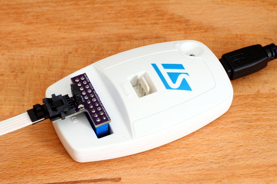
An open-source SWD programming adapter showcasing its simple, low-pin-count connection.
Performance and Debugging Speed
For flashing firmware and routine debugging tasks, SWD typically offers better performance on modern debugging tools. Sources indicate that JTAG performance on specific programmers like MiniProg4 may be significantly slower than SWD, particularly for operations like flash programming and real-time debugging. This efficiency can lead to reduced development cycles and faster iteration times, which are invaluable during software development and testing.
Deep Sleep Mode Accessibility
The PSoC 62's ability to maintain SWD access during Deep-Sleep mode is a critical advantage for power-optimized designs. JTAG pins, conversely, are generally not accessible in this low-power state. This allows developers to debug power-saving routines and transient issues without compromising the device's sleep functionality.
Toolchain Compatibility and Default Settings
Modern development environments and debuggers, including Infineon's ModusToolbox and PSoC Creator, are well-optimized for SWD. Many development kits, such as the CY8CKIT-062S4 Pioneer Kit, come with onboard debuggers (e.g., KitProg3) that default to SWD for efficient programming and debugging. While both protocols are configurable within the IDEs, SWD is often the default and recommended choice for its simplicity and direct integration with ARM Cortex-M based MCUs like the PSoC 62.
Comparison Table: SWD vs. JTAG for PSoC 62
The table below summarizes the key distinctions and advantages of each protocol in the context of the Infineon PSoC 62 device.
| Feature | SWD (Serial Wire Debug) | JTAG (Joint Test Action Group) |
|---|---|---|
| Pins Required | 2 (SWDIO, SWCLK) + GND, Reset | 4-5 (TCK, TMS, TDI, TDO, TRST) + GND, Reset |
| Hardware Complexity | Lower, simpler PCB routing | Higher, more complex PCB routing |
| Debugging Speed | Generally faster for flash programming & debug cycles | Can be slower on some tools (e.g., MiniProg4) |
| Multi-Device Support | No direct daisy-chaining | Yes, supports daisy-chaining multiple devices |
| Deep Sleep Debug | Pins remain active, enabling debug | Pins generally inaccessible |
| Primary Use Case | Most embedded development, single-chip debugging | Advanced test, boundary scan, multi-chip systems |
| Power Efficiency | Lower susceptibility to noise, beneficial for IoT | Higher pin count can increase noise potential |
Visualizing Debugging Protocol Characteristics
To further illustrate the practical implications of choosing between SWD and JTAG for the PSoC 62, the following radar chart provides an opinionated analysis of their respective strengths across various relevant criteria.
This radar chart illustrates that SWD generally scores higher in aspects crucial for typical PSoC 62 embedded development, such as pin efficiency, debugging speed, and deep sleep debugging capabilities. JTAG, while strong in multi-chip capabilities, lags in other areas important for common PSoC 62 applications.
Navigating the PSoC 62 Debugging Ecosystem
Infineon provides robust support for both SWD and JTAG within its development ecosystem. Integrated Development Environments (IDEs) and debugging tools offer seamless integration for either protocol.
ModusToolbox™ and PSoC Creator
Both ModusToolbox™ and PSoC Creator are powerful software suites recommended for developing and debugging PSoC 6 MCU projects. They enable comprehensive configuration of device resources, middleware libraries, and support writing C/assembly code. Within these IDEs, the debug port (JTAG or SWD) can be easily selected via the system editor or debug configuration settings. This flexibility ensures developers can choose the interface that best suits their project's requirements.
The "Welcome to Modus Toolbox: #4 Program & Debug" video explains the debugging options available within ModusToolbox, highlighting the support for various debugger hardware and configurations for your PSoC 62 projects.
Third-Party Probes and Debuggers
The PSoC 62's Debug Access Port (DAP) supports industry-standard third-party probes and debuggers, including J-Link and OpenOCD. These tools provide flash programming capabilities and GDB server functionality for debugging. By default, OpenOCD often utilizes the SWD protocol, though JTAG can be enabled with specific commands in the Debug Configuration if required for particular scenarios.
Decision Framework: Choosing the Right Protocol
The optimal choice between SWD and JTAG for your Infineon PSoC 62 device depends on your project's specific requirements, constraints, and the debugging capabilities you need.
This mindmap visually outlines the decision-making process, highlighting the strengths and typical applications for both SWD and JTAG. For the vast majority of PSoC 62 projects involving single-chip development and general debugging, SWD remains the superior choice due to its efficiency and simplicity. However, if your application necessitates advanced boundary scan testing, debugging of multiple chained devices, or integration with existing legacy JTAG-centric systems, then JTAG might be a more suitable, albeit often slower, alternative.
Frequently Asked Questions (FAQ)
What is the primary advantage of SWD over JTAG for PSoC 62?
Can I switch between SWD and JTAG on a PSoC 62 device?
Does SWD support multi-core debugging on PSoC 62?
Are there any scenarios where JTAG is still preferred for PSoC 62?
Does using SWD impact power consumption on PSoC 62?
Conclusion
For flashing and debugging the Infineon PSoC 62 device, SWD (Serial Wire Debug) is generally the superior choice. Its minimal pin requirements, often higher performance in modern toolchains, and ability to remain active in Deep-Sleep mode make it ideal for the power-efficient and compact designs often associated with PSoC 62 MCUs. While JTAG (Joint Test Action Group) offers advanced multi-chip testing capabilities and is fully supported by the PSoC 62 platform, its increased pin count and potentially slower performance make it less practical for most general embedded development tasks. Ultimately, the decision should align with your specific project needs, prioritizing SWD for streamlined and efficient development unless explicit requirements for JTAG's unique features dictate otherwise.
Recommended Further Exploration
- How to configure PSoC 62 for SWD debugging in ModusToolbox
- Advanced JTAG features for complex PSoC 62 systems
- Debugging low-power modes on Infineon PSoC 62 with SWD
- Troubleshooting common PSoC 62 flashing and debugging issues