
Understanding Scanning Transmission Electron Microscopy (STEM)
A Comprehensive Baseline Explanation for Beginners
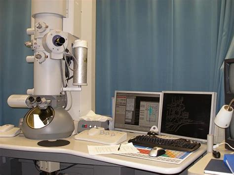
Key Takeaways
- STEM Integration of TEM and SEM: Combines the high-resolution imaging capabilities of Transmission Electron Microscopy (TEM) with the surface analysis strengths of Scanning Electron Microscopy (SEM).
- Atomic-Scale Resolution: Achieves sub-atomic resolution, allowing for detailed visualization of materials at the nanometer and sub-nanometer levels.
- Versatile Applications: Utilized across various fields, including materials science, nanotechnology, biology, and semiconductor research, for both imaging and compositional analysis.
Introduction to STEM
Scanning Transmission Electron Microscopy (STEM) is a sophisticated imaging technique that merges the functionalities of Transmission Electron Microscopy (TEM) and Scanning Electron Microscopy (SEM). By utilizing a focused beam of electrons, STEM allows scientists to explore the internal structures and compositions of materials at unprecedented resolutions, ranging from nanometers to sub-atomic scales.
Basic Principles of STEM
How STEM Operates
STEM operates by directing a finely focused, high-energy electron beam onto an ultrathin sample. As the electron beam interacts with the sample, various signals are generated, including transmitted electrons, scattered electrons, and characteristic X-rays. These signals are then captured by different detectors to form detailed images and perform compositional analyses.
Electron Beam Generation and Focusing
The electron beam in STEM is generated using a high-quality electron source, typically a field emission gun (FEG). This source produces a coherent and highly focused beam, which is then manipulated using electromagnetic lenses to form a fine probe. With the aid of aberration correctors, the probe size can be reduced to less than 100 picometers, enabling atomic-scale resolution.
Scanning Mechanism
Unlike conventional TEM, which illuminates the entire sample simultaneously, STEM scans the electron beam in a raster pattern, point by point. This scanning process allows for precise control over the area being imaged and facilitates the collection of various types of data simultaneously.
Key Components of STEM
Electron Source
The electron source is fundamental to STEM's operation, generating a high-energy electron beam necessary for deep penetration into the sample. Field emission guns are preferred for their ability to produce a stable and coherent beam, essential for high-resolution imaging.
Electron Optical System
The electron optical system comprises electromagnetic lenses that focus and control the electron beam's convergence and divergence. Advanced aberration correctors are employed to minimize lens imperfections, thereby enhancing the system's overall resolution and image quality.
Sample Stage
The sample is placed on a stage that can be precisely controlled in three dimensions. This stage allows for the tilting, rotating, and translating of the sample to capture images from various angles and positions, providing a comprehensive view of the material's structure.
Detectors
STEM utilizes multiple detectors to capture different signals generated during electron-sample interactions:
- Bright-Field (BF) Detector: Captures electrons that pass through the sample with minimal scattering, highlighting areas based on mass and thickness.
- Dark-Field (DF) Detector: Collects electrons scattered at high angles, revealing structural details like defects and crystal orientations.
- High-Angle Annular Dark-Field (HAADF) Detector: Sensitive to atomic number differences, providing Z-contrast imaging to distinguish elements based on their atomic weights.
- Spectroscopic Detectors: Include Energy-Dispersive X-ray Spectroscopy (EDS) and Electron Energy Loss Spectroscopy (EELS) for elemental and chemical analysis.
Sample Preparation for STEM
Importance of Thin Samples
For effective STEM imaging, samples must be extremely thin, typically less than 100 nanometers thick. This thinness ensures that electrons can transmit through the sample with minimal scattering, which is crucial for obtaining clear and high-resolution images.
Preparation Techniques
Preparing samples for STEM involves several sophisticated methods to achieve the required thinness without introducing artifacts:
-
Ion Milling: Utilizes ions to progressively thin the sample material.
-
Focused Ion Beam (FIB) Milling: A more precise method where a focused ion beam sculpts the sample at the nanoscale.
-
Ultra-Fine Slicing: Achieved using specialized ultramicrotomes to slice thin sections with high precision.
Avoiding Sample Artifacts
Proper sample preparation is critical to prevent distortions and artifacts that can compromise the accuracy of STEM analyses. Techniques must be carefully selected and executed to maintain the sample's integrity and represent its true structure.
Imaging and Analysis Modes in STEM
Bright-Field (BF) and Dark-Field (DF) Imaging
BF imaging in STEM captures electrons that pass directly through the sample, providing images where contrast is based on the sample's mass and thickness. DF imaging, on the other hand, collects electrons that are scattered to higher angles, highlighting structural features like grain boundaries, defects, and crystallographic orientations.
High-Angle Annular Dark-Field (HAADF) Imaging
HAADF imaging offers Z-contrast, where the image intensity correlates with the atomic number of the elements in the sample. This mode is particularly useful for distinguishing between elements with different atomic weights, allowing for precise elemental mapping and identification within the material.
Electron Energy Loss Spectroscopy (EELS)
EELS measures the energy lost by electrons as they pass through the sample, providing detailed information about the sample's elemental composition and electronic structure. This spectroscopic technique enables the identification of elements and analysis of chemical bonding and electronic transitions.
Energy-Dispersive X-ray Spectroscopy (EDS)
EDS detects characteristic X-rays emitted from the sample when it is bombarded by the electron beam. By analyzing these X-rays, EDS can determine the elemental composition of specific areas within the sample, complementing the imaging capabilities of STEM.
Differential Phase Contrast (DPC) Imaging
DPC imaging provides contrast based on the phase shifts of the electron beam as it passes through the sample. This mode is effective for visualizing electric and magnetic fields within the sample, offering insights into its internal electronic structure.
Applications of STEM
Materials Science
In materials science, STEM is invaluable for analyzing the microstructure of metals, ceramics, and polymers. It enables the study of grain boundaries, defects, phase distributions, and the arrangement of atoms within crystal lattices.
Nanotechnology
STEM facilitates the characterization of nanoparticles, nanowires, and other nanostructures. Its high resolution allows for the examination of size, shape, composition, and structural integrity at the nanoscale.
Biological Sciences
In biology, STEM is used to image cellular structures, macromolecules, and viruses with high precision. It provides detailed views of biological specimens, contributing to our understanding of their morphology and composition.
Semiconductor Industry
For semiconductor research and development, STEM is essential in analyzing defects, interfaces, and doping distributions within electronic devices. It aids in optimizing the performance and reliability of semiconductor materials.
Chemical Composition Mapping
STEM's ability to perform simultaneous imaging and spectroscopic analysis makes it ideal for mapping the distribution of elements and compounds within complex materials, providing insights into their chemical homogeneity and interactions.
Advantages of STEM
Exceptional Resolution
STEM achieves sub-atomic resolution, allowing scientists to visualize individual atoms and their arrangements within materials. This level of detail surpasses that of many other imaging techniques, making STEM indispensable for atomic-scale research.
Multifaceted Analytical Capabilities
Beyond imaging, STEM's integration of spectroscopy techniques like EELS and EDS enables comprehensive analysis of both the structure and composition of samples. This dual capability provides a holistic understanding of material properties.
Quantitative Analysis
STEM allows for precise measurements of atomic positions, interatomic distances, and elemental concentrations. This quantitative data is crucial for validating theoretical models and understanding material behavior at the nanoscale.
Versatility Across Disciplines
The diverse applications of STEM across various scientific fields highlight its versatility. Whether in materials science, biology, or electronics, STEM provides critical insights that drive innovation and discovery.
Challenges and Limitations
Sample Preparation Complexity
Preparing ultrathin samples without introducing artifacts is a technically demanding process. Achieving the necessary sample thickness while maintaining structural integrity requires specialized equipment and expertise.
Environmental Sensitivity
STEM requires a vibration-free environment and stable temperature conditions to maintain high-resolution imaging. External disturbances can degrade image quality, necessitating controlled laboratory settings.
High Operational Costs
STEM instruments are sophisticated and expensive, both in terms of initial investment and maintenance. Additionally, operating STEM typically requires highly trained personnel, contributing to the overall cost.
Beam-Induced Sample Damage
The high-energy electron beam can cause damage to sensitive samples, such as biological specimens or certain nanomaterials. Mitigating beam-induced damage requires careful adjustment of imaging parameters and sometimes cryogenic techniques.
Future Directions in STEM
Advancements in Aberration Correction
Ongoing improvements in aberration correction technologies continue to enhance STEM's resolution and image quality. These advancements allow for even finer probing of material structures, pushing the boundaries of atomic-scale imaging.
Integration with Other Analytical Techniques
Future developments aim to integrate STEM with other analytical modalities, such as in-situ testing and 3D tomography. These integrations will provide more comprehensive insights into material behaviors under various conditions.
Automation and Machine Learning
The incorporation of automation and machine learning algorithms into STEM workflows promises to streamline data acquisition and analysis. Automated systems can enhance efficiency and reduce the potential for human error, facilitating large-scale studies.
Conclusion
Scanning Transmission Electron Microscopy (STEM) stands as a pinnacle of modern imaging techniques, offering unparalleled insights into the structure and composition of materials at the atomic level. Its integration of TEM and SEM capabilities, combined with advanced spectroscopic analysis, makes STEM an indispensable tool across multiple scientific disciplines. Despite its challenges, ongoing technological advancements continue to expand its applications and effectiveness, ensuring its critical role in future scientific discoveries and technological innovations.
References
Last updated January 20, 2025