
Synthesizable SystemVerilog AXI4 Bus Example Using Interface Object
A Comprehensive Guide to Implementing AXI4 Communication in SystemVerilog
Key Takeaways
- Modular Design: SystemVerilog interfaces encapsulate AXI4 signals for easy reuse.
- Synthesizable Code: Adheres to synthesizable coding practices essential for FPGA/ASIC implementation.
- Comprehensive Example: Includes master, slave modules, and testbench for complete AXI4 communication.
Introduction
The Advanced eXtensible Interface 4 (AXI4) protocol is a cornerstone in modern on-chip communication, particularly within ARM-based systems. SystemVerilog, with its robust features, offers a streamlined approach to implementing AXI4 through the use of interfaces. This not only promotes modularity and reusability but also simplifies the complex signal interactions inherent in AXI4 communication.
In this guide, you'll find a detailed example of a synthesizable SystemVerilog AXI4 bus using an interface object. The example encompasses the definition of the AXI4 interface, master and slave modules, a top-level module, and a testbench to simulate and verify the communication.
AXI4 Interface Definition
Defining an AXI4 interface in SystemVerilog serves as the foundation for establishing communication between master and slave modules. The interface encapsulates all necessary signals across the five AXI4 channels: Write Address (AW), Write Data (W), Write Response (B), Read Address (AR), and Read Data (R).
// AXI4 Interface Definition
interface axi4_if #(
    parameter ID_WIDTH = 4,
    parameter ADDR_WIDTH = 32,
    parameter DATA_WIDTH = 32
)(
    input logic clk,
    input logic rst_n
);

// Write Address Channel
logic [ID_WIDTH-1:0] awid;
logic [ADDR_WIDTH-1:0] awaddr;
logic [7:0] awlen;
logic [2:0] awsize;
logic [1:0] awburst;
logic awvalid;
logic awready;

// Write Data Channel
logic [DATA_WIDTH-1:0] wdata;
logic [DATA_WIDTH/8-1:0] wstrb;
logic wlast;
logic wvalid;
logic wready;

// Write Response Channel
logic [ID_WIDTH-1:0] bid;
logic [1:0] bresp;
logic bvalid;
logic bready;

// Read Address Channel
logic [ID_WIDTH-1:0] arid;
logic [ADDR_WIDTH-1:0] araddr;
logic [7:0] arlen;
logic [2:0] arsize;
logic [1:0] arburst;
logic arvalid;
logic arready;

// Read Data Channel
logic [ID_WIDTH-1:0] rid;
logic [DATA_WIDTH-1:0] rdata;
logic [1:0] rresp;
logic rlast;
logic rvalid;
logic rready;

// Modports for directionality
modport master (
    input clk, rst_n,
    // Write Address
    output awid, awaddr, awlen, awsize, awburst, awvalid,
    input awready,
    // Write Data
    output wdata, wstrb, wlast, wvalid,
    input wready,
    // Write Response
    input [bid, bresp, bvalid],
    output bready,
    // Read Address
    output arid, araddr, arlen, arsize, arburst, arvalid,
    input arready,
    // Read Data
    input [rid, rdata, rresp, rlast, rvalid],
    output rready
);

modport slave (
    input clk, rst_n,
    // Write Address
    input awid, awaddr, awlen, awsize, awburst, awvalid,
    output awready,
    // Write Data
    input wdata, wstrb, wlast, wvalid,
    output wready,
    // Write Response
    output [bid, bresp, bvalid],
    input bready,
    // Read Address
    input arid, araddr, arlen, arsize, arburst, arvalid,
    output arready,
    // Read Data
    output [rid, rdata, rresp, rlast, rvalid],
    input rready
);

endinterface
Explanation
- Parameterized Interface: The interface is parameterized with
ID_WIDTH,ADDR_WIDTH, andDATA_WIDTHto allow flexibility in different designs. - Signal Definitions: All AXI4 channel signals are defined within the interface, ensuring a consolidated and organized structure.
- Modports: Separate modports for
masterandslavedefine the directionality of signals, facilitating clear communication roles.
Master Module Example
The master module initiates read and write transactions. Below is an example of a simplified AXI4 master that performs a write and a read operation.
// AXI4 Master Module
module axi4_master #(
    parameter ID_WIDTH = 4,
    parameter ADDR_WIDTH = 32,
    parameter DATA_WIDTH = 32
)(
    axi4_if.master axi
);

    // Initial Write Operation
    initial begin
        // Reset
        @(posedge axi.clk);
        axi.awvalid <= 1'b0;
        axi.wvalid  <= 1'b0;
        axi.bready  <= 1'b0;
        axi.arvalid <= 1'b0;
        axi.rready  <= 1'b0;

        // Wait for reset de-assertion
        wait (axi.rst_n == 1);

        // Write Address Channel
        @(posedge axi.clk);
        axi.awid    <= 4'd1;
        axi.awaddr  <= 32'h0000_1000;
        axi.awlen   <= 8'd0;
        axi.awsize  <= 3'd2; // 4 bytes
        axi.awburst <= 2'd0; // Fixed burst
        axi.awvalid <= 1'b1;

        // Write Data Channel
        @(posedge axi.clk);
        axi.wdata  <= 32'hDEAD_BEEF;
        axi.wstrb  <= 4'b1111;
        axi.wlast  <= 1'b1;
        axi.wvalid <= 1'b1;

        // Wait for write response
        @(posedge axi.clk);
        axi.bready <= 1'b1;
        @(posedge axi.clk);
        axi.awvalid <= 1'b0;
        axi.wvalid  <= 1'b0;
        axi.bready  <= 1'b0;

        // Read Address Channel
        @(posedge axi.clk);
        axi.arid    <= 4'd1;
        axi.araddr  <= 32'h0000_1000;
        axi.arlen   <= 8'd0;
        axi.arsize  <= 3'd2; // 4 bytes
        axi.arburst <= 2'd0; // Fixed burst
        axi.arvalid <= 1'b1;

        // Read Data Channel
        @(posedge axi.clk);
        axi.rready  <= 1'b1;
        @(posedge axi.clk);
        axi.arvalid <= 1'b0;
        axi.rready  <= 1'b0;
    end
endmodule
Explanation
- Initialization: The master initializes the AXI4 signals to their default states and waits for the reset to be de-asserted.
- Write Operation:
- The master sets up the write address and asserts
awvalid. - It then provides the write data and asserts
wvalid. - Upon receiving the write response, it asserts
breadyto acknowledge the response.
- The master sets up the write address and asserts
- Read Operation:
- The master sets up the read address and asserts
arvalid. - It then asserts
rreadyto receive the read data.
- The master sets up the read address and asserts
Slave Module Example
The slave module responds to the master's read and write requests. Below is a simple AXI4 slave that writes data to a memory array and reads data from it.
// AXI4 Slave Module
module axi4_slave #(
    parameter ID_WIDTH = 4,
    parameter ADDR_WIDTH = 32,
    parameter DATA_WIDTH = 32
)(
    axi4_if.slave axi
);
    // Memory Array
    reg [DATA_WIDTH-1:0] memory [0:1023];

    // Write Address and Data Handlers
    always @(posedge axi.clk or negedge axi.rst_n) begin
        if (!axi.rst_n) begin
            axi.awready <= 1'b0;
            axi.wready  <= 1'b0;
            axi.bvalid  <= 1'b0;
        end else begin
            // Write Address Handshake
            if (axi.awvalid && !axi.awready) begin
                axi.awready <= 1'b1;
            end else begin
                axi.awready <= 1'b0;
            end

            // Write Data Handshake
            if (axi.wvalid && !axi.wready) begin
                axi.wready <= 1'b1;
                memory[axi.awaddr] <= axi.wdata;
            end else begin
                axi.wready <= 1'b0;
            end

            // Write Response
            if (axi.awready && axi.wready && !axi.bvalid) begin
                axi.bvalid  <= 1'b1;
                axi.bresp   <= 2'b00; // OKAY response
                axi.bid     <= axi.awid;
            end else if (axi.bvalid && axi.bready) begin
                axi.bvalid <= 1'b0;
            end
        end
    end

    // Read Address and Data Handlers
    always @(posedge axi.clk or negedge axi.rst_n) begin
        if (!axi.rst_n) begin
            axi.arready <= 1'b0;
            axi.rvalid  <= 1'b0;
            axi.rdata   <= {DATA_WIDTH{1'b0}};
            axi.rid     <= {ID_WIDTH{1'b0}};
            axi.rresp   <= 2'b00;
        end else begin
            // Read Address Handshake
            if (axi.arvalid && !axi.arready) begin
                axi.arready <= 1'b1;
                axi.rdata   <= memory[axi.araddr];
                axi.rid     <= axi.arid;
            end else begin
                axi.arready <= 1'b0;
            end

            // Read Data Response
            if (axi.arready && !axi.rvalid) begin
                axi.rvalid <= 1'b1;
                axi.rresp  <= 2'b00; // OKAY response
                axi.rlast  <= 1'b1;   // Single beat
            end else if (axi.rvalid && axi.rready) begin
                axi.rvalid <= 1'b0;
            end
        end
    end
endmodule
Explanation
- Memory Array: A simple memory array is defined to store and retrieve data based on the address.
- Write Handlers:
awreadyandwreadyare asserted to acknowledge the write address and data.- Data is written to the memory array when both
awvalidandwvalidare high. - A write response is then generated by asserting
bvalid.
- Read Handlers:
arreadyis asserted to acknowledge the read address.- Data is read from the memory array and placed on
rdata. - A read response is generated by asserting
rvalid.
Top-Level Module
The top-level module instantiates both the master and slave modules and connects them via the AXI4 interface. It also generates the necessary clock and reset signals.
// Top-Level Module
module top;
    // Clock and Reset Signals
    logic clk;
    logic rst_n;

    // Instantiate AXI4 Interface
    axi4_if #(
        .ID_WIDTH(4),
        .ADDR_WIDTH(32),
        .DATA_WIDTH(32)
    ) axi_bus (
        .clk(clk),
        .rst_n(rst_n)
    );

    // Instantiate Master and Slave Modules
    axi4_master #(
        .ID_WIDTH(4),
        .ADDR_WIDTH(32),
        .DATA_WIDTH(32)
    ) master_inst (
        .axi(axi_bus.master)
    );

    axi4_slave #(
        .ID_WIDTH(4),
        .ADDR_WIDTH(32),
        .DATA_WIDTH(32)
    ) slave_inst (
        .axi(axi_bus.slave)
    );

    // Clock Generation
    initial begin
        clk = 0;
        forever #5 clk = ~clk; // 100 MHz Clock
    end

    // Reset Generation
    initial begin
        rst_n = 0;
        #20 rst_n = 1;
    end
endmodule
Explanation
- Signal Generation: The top module generates the clock (
clk) and reset (rst_n) signals required by the AXI4 interface. - Interface Instantiation: An instance of the
axi4_ifinterface is created with specified parameters. - Module Instantiation: Both the master and slave modules are instantiated and connected to the interface via their respective modports.
Testbench Example
The testbench is essential for verifying the functionality of the AXI4 communication between the master and slave modules. It simulates the reset behavior and monitors the transactions.
// AXI4 Testbench
module testbench;
    // Instantiate Top-Level Module
    top uut ();

    // Simulation Duration
    initial begin
        // Run simulation for 200 time units
        #200;
        $stop;
    end
endmodule
Explanation
- Instantiation: The testbench instantiates the top-level module, which in turn instantiates the master, slave, and AXI4 interface.
- Simulation Control: The simulation is set to run for a predefined duration (e.g., 200 time units) before stopping.
- Monitoring: During simulation, waveform viewers can be used to observe the signal transitions and verify correct behavior of read and write operations.
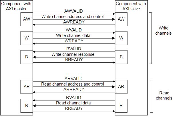
AXI4 Channels Overview
Understanding the AXI4 channels is crucial for implementing effective communication between master and slave devices. Below is a summary of each channel and its primary functions.
| Channel | Purpose |
|---|---|
| AW (Write Address) | Specifies the address and control information for write transactions. |
| W (Write Data) | Transfers the actual data to be written to the slave. |
| B (Write Response) | Provides feedback from the slave regarding the write transaction status. |
| AR (Read Address) | Specifies the address and control information for read transactions. |
| R (Read Data) | Transfers the requested data from the slave to the master. |
Best Practices for Synthesizable AXI4 Design
When designing synthesizable AXI4 modules in SystemVerilog, adhering to best practices ensures reliability and efficiency. Here are some key considerations:
-
Clock Domain Management: Ensure that all AXI4 signals are synchronized to the same clock domain to prevent metastability.
-
Reset Synchronization: Properly handle reset signals to initialize AXI4 channels and internal states.
-
Parameterization: Utilize parameters for address width, data width, and ID width to enhance the scalability and reusability of the modules.
-
Handshaking Mechanisms: Correctly implement the handshaking signals (
validandready) to manage data flow control. -
Error Handling: Incorporate error response mechanisms to handle exceptional conditions gracefully.
-
Timing Constraints: Adhere to timing requirements specified by the AXI4 protocol to ensure reliable data transfers.
Conclusion
This comprehensive example illustrates how to implement a synthesizable SystemVerilog AXI4 bus using an interface object. By encapsulating AXI4 signals within a SystemVerilog interface, designers can create modular and reusable components that streamline the development process. The provided master and slave modules, along with the top-level module and testbench, offer a solid foundation for building and verifying complex AXI4-based systems.
Adhering to best practices in AXI4 design ensures that the resulting modules are robust, efficient, and ready for integration into larger FPGA or ASIC designs.
References
These resources provide additional insights and examples to deepen your understanding of AXI4 and SystemVerilog interface implementations.
Last updated January 24, 2025