
Impact of Larger Via1 Critical Dimension (CD) Compared to M1 in Semiconductor Manufacturing
Understanding the Consequences of Via1 CD Oversizing on Via1 Width and M1 Alignment Integrity
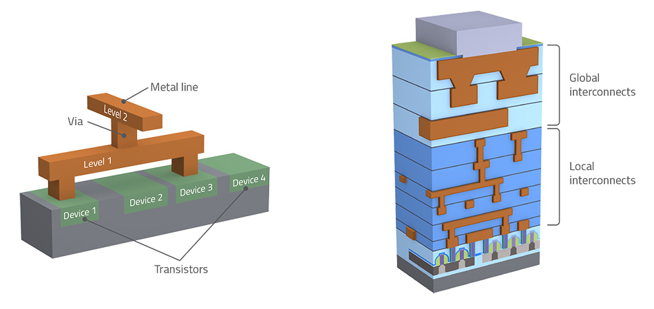
Key Takeaways
- Increased Misalignment Risks: A larger Via1 CD compared to M1 heightens the potential for misalignment, leading to compromised electrical connections.
- Reduced Electrical Performance: Oversized Via1 can cause width loss and heightened electrical resistance, negatively affecting device reliability.
- Enhanced Process Complexity: Managing discrepancies between Via1 CD and M1 requires stringent process controls and advanced calibration techniques.
1. Critical Dimension (CD) Mismatch: Via1 vs. M1
Understanding Critical Dimensions in Semiconductor Layers
In semiconductor manufacturing, the Critical Dimension (CD) refers to the precise width of a feature within a specific layer of an integrated circuit. The Via1 layer is responsible for creating vertical connections between different metal layers, while the Metal-1 (M1) layer constitutes the primary horizontal wiring that forms the circuit pathways.
Implications of Via1 CD Being Larger Than M1 CD
When the Via1 CD exceeds the M1 CD, it introduces several critical issues that can significantly impact the overall performance and yield of semiconductor devices:
a. Width Loss in Via1 (W)
An oversized Via1 CD means that the via extends beyond the intended boundaries of the M1 landing pad. This overextension can result in incomplete or inadequate contact between the Via1 and M1 layers, leading to a reduction in the effective width of the via. Consequently, the electrical connectivity can deteriorate, increasing the contact resistance and potentially causing intermittent faults or complete open circuits.
b. M1 Alignment Integrity (AI) Loss
The alignment integrity between Via1 and M1 is crucial for ensuring reliable electrical connections. A larger Via1 CD exacerbates the risk of misalignment, where the via may not align perfectly with the M1 trace. Such misalignments can lead to open circuits, increased electrical resistance, and reduced overall device reliability. The Alignment and Lithography Feedback (ALF) system, which monitors and corrects alignment errors during the manufacturing process, may struggle to compensate for significant CD mismatches, thereby compounding the alignment issues.
c. Increased Electrical Resistance
With the effective width of Via1 compromised, the pathway for electrical current becomes narrower. This limitation increases the electrical resistance at the connection point, which can lead to signal degradation, slower switching speeds, and higher power consumption. In high-performance or high-frequency applications, such increased resistance can severely impact the functionality and efficiency of the semiconductor device.
d. Electromigration and Reliability Concerns
Electromigration, the gradual movement of metal atoms due to high current densities, becomes a significant concern when Via1 CD is larger than M1. The reduced contact area and increased current density can accelerate electromigration, leading to void formation or hillock growth. These physical changes compromise the structural integrity of the connections, resulting in reduced device lifespan and increased failure rates.
2. Alignment and Lithography Feedback (ALF) Component
Role of ALF in Semiconductor Manufacturing
The Alignment and Lithography Feedback (ALF) system is integral to maintaining precision during the photolithography process. It continuously monitors alignment parameters and provides real-time adjustments to counteract any deviations or errors that occur during layer patterning.
Challenges Faced by ALF with Oversized Via1 CD
When the Via1 CD is larger than the M1 CD, the ALF system encounters several challenges:
a. Exceeding ALF Tolerance Limits
ALF systems operate within specific tolerance ranges to correct alignment errors. A significant CD mismatch pushes the alignment beyond these predefined tolerances, rendering the ALF less effective or even ineffective in compensating for the misalignment. This limitation means that even minute shifts can lead to substantial alignment errors that the ALF cannot rectify.
b. Increased Error Magnitude
The disparity between the Via1 and M1 CDs amplifies the alignment errors, making it more difficult for the ALF to make precise adjustments. Larger errors can accumulate over successive layers, leading to compounded misalignments that degrade the overall device performance and yield.
c. Feedback Loop Instability
Excessive CD mismatches can lead to instability in the feedback loop of the ALF system. The system might oscillate trying to correct errors that are beyond its operational capacity, resulting in further misalignments and increased defect rates.
3. Root Causes of Via1 CD Oversizing
a. Process Variability
Manufacturing processes inherently involve variations due to factors such as temperature fluctuations, equipment precision, and material inconsistencies. Variability in etching or deposition processes can lead to unintended expansions of the Via1 CD. For example, over-etching during via formation can inadvertently increase the Via1 CD beyond the intended specifications, causing mismatches with the M1 layer.
b. Design Rule Violations
Strict adherence to design rules is paramount in semiconductor manufacturing. Design rule violations, such as incorrect pitch or spacing between M1 and Via1 layers, can result in improper alignment and CD mismatches. Inadequate design considerations may not account for process variations, leading to oversized vias that do not align correctly with the M1 traces.
c. Material and Lithography Challenges
Advanced semiconductor nodes employ materials like tungsten or copper for vias and metal layers. These materials present their own set of challenges, such as increased resistance and difficulties in achieving uniform gapfill. Additionally, as feature sizes shrink, lithographic precision becomes critical. Any imperfections in patterning or etching can disproportionately affect the Via1 CD, making it challenging to maintain consistent alignment with the M1 layer.
d. Aspect Ratio Limitations
High aspect ratio vias, where the height significantly exceeds the width, complicate the manufacturing process. Achieving uniform fill without voids or seams becomes more difficult as the aspect ratio increases, making it harder to control the Via1 CD precisely. This can result in larger via dimensions that do not align well with narrower M1 traces.
4. Implications on Semiconductor Device Performance
a. Electrical Connectivity Issues
Proper electrical connectivity between the Via1 and M1 layers is essential for reliable device operation. An oversized Via1 CD can lead to insufficient or inconsistent contact points, increasing the likelihood of open circuits or high-resistance pathways. These electrical connectivity issues can manifest as functional failures, signal integrity problems, or reduced performance in the final device.
b. Yield Loss and Defect Increase
Misalignments and connectivity issues directly contribute to lower manufacturing yields. Devices with defective vias or poor electrical connections are typically culled during testing, reducing the overall yield of the manufacturing process. Additionally, increased defect rates elevate production costs and prolong time-to-market for semiconductor products.
c. Enhanced Electromigration Risks
Electromigration, driven by high current densities, can degrade metal lines and vias over time. An oversized Via1 CD concentrates current flow, exacerbating electromigration effects. This acceleration can lead to the formation of voids and hillocks within the metal, compromising the structural integrity and longevity of the connections.
d. Thermal Management Challenges
Electrical resistance introduced by Via1 CD mismatches results in localized heating, which can adversely affect device performance and reliability. Excessive heat may necessitate more robust thermal management solutions, adding complexity and cost to the semiconductor manufacturing process.
5. Mitigation Strategies
a. Optimize Via1 CD to Match M1
Ensuring that the Via1 CD is equal to or smaller than the M1 CD is fundamental. This requires precise control over the etching and deposition processes to maintain consistent via dimensions. Utilizing advanced lithography techniques and high-precision equipment can help achieve the desired Via1 CD.
b. Implement Rigorous Design Rule Checks (DRC)
Adhering strictly to design rules is critical for maintaining alignment integrity. Incorporating comprehensive Design Rule Checks (DRC) into the design and verification stages ensures that Via1 and M1 layers comply with the specified pitch and spacing guidelines. Automated DRC tools can identify potential mismatches early in the design process, allowing for corrective measures before fabrication.
c. Advanced ALF Calibration and Enhancement
Enhancing the calibration of the ALF system to account for potential misalignments caused by larger Via1 CDs can improve its compensatory capabilities. This involves refining the feedback algorithms and expanding the operational tolerance ranges of the ALF system to better handle deviations, thereby reducing the likelihood of alignment errors.
d. Utilize Redundant Via Insertion
Incorporating redundant vias provides alternative electrical pathways, enhancing the reliability and yield of semiconductor devices. Redundant vias can compensate for potential failures or insufficient contacts caused by CD mismatches, ensuring that the device maintains its electrical performance even in the presence of alignment discrepancies.
e. Employ Self-Aligned Via Techniques
Advanced self-aligned via (SAV) technologies automate the alignment process, reducing the dependency on manual calibration and minimizing the risk of misalignment. SAV techniques leverage precise patterning and alignment mechanisms to ensure that vias are accurately positioned relative to metal layers, maintaining consistent CD ratios.
f. Enhanced Process Control and Monitoring
Implementing stringent process control measures and continuous monitoring throughout the manufacturing process can help detect and mitigate CD mismatches in real-time. Utilizing in-line metrology tools to monitor via and metal dimensions ensures that any deviations are promptly addressed, maintaining the integrity of the semiconductor device.
6. Advanced Techniques for Maintaining CD Consistency
a. Chemical Mechanical Planarization (CMP)
CMP is a critical process that ensures flatness and uniformity across the wafer surface by polishing the layers to precise thicknesses. Effective CMP can help maintain consistent Via1 and M1 CDs by removing excess material and minimizing topographical variations that contribute to misalignment.
b. High-Resolution Lithography
Employing high-resolution lithography techniques, such as Extreme Ultraviolet (EUV) lithography, allows for more precise patterning of vias and metal layers. This precision reduces the likelihood of CD mismatches and enhances the overall alignment between different layers, ensuring that Via1 CD remains proportionate to M1 CD.
c. Metrology and Inspection Enhancements
Integrating advanced metrology and inspection systems provides real-time feedback on CD dimensions and alignment accuracy. Techniques like Scanning Electron Microscopy (SEM) and Atomic Force Microscopy (AFM) offer detailed insights into feature dimensions, enabling proactive adjustments to manufacturing processes.
d. Adaptive Process Controls
Adaptive process controls leverage machine learning and artificial intelligence to optimize manufacturing parameters dynamically. By analyzing data from various process steps, adaptive controls can predict and correct potential CD mismatches before they impact the final device, maintaining consistent Via1 and M1 dimensions.
e. Material Innovation
Developing and utilizing advanced materials with superior etching and deposition characteristics can facilitate more precise control over Via1 and M1 CDs. Innovations in low-k dielectrics and barrier metals contribute to better alignment and reduced variability during the manufacturing process.
7. Comprehensive Impact on Semiconductor Manufacturing
a. Enhanced Device Performance
Maintaining consistent Via1 and M1 CDs ensures reliable electrical connections, which directly translates to enhanced device performance. Reduced electrical resistance and minimized alignment errors result in faster switching speeds, lower power consumption, and higher overall efficiency of semiconductor devices.
b. Improved Yield and Cost Efficiency
Addressing CD mismatches through optimized manufacturing processes and advanced techniques leads to higher yields by minimizing defects and failures. Improved yields reduce the cost per device, making semiconductor manufacturing more economically viable and competitive.
c. Reliability and Longevity
Consistent Via1 and M1 dimensions enhance the structural integrity of electrical connections, mitigating risks related to electromigration and thermal stress. Reliable connections ensure longer device lifespans and reduce the likelihood of field failures, which is vital for critical applications in electronics and computing.
d. Scalability for Advanced Nodes
As semiconductor technology advances towards smaller nodes, maintaining precise CD ratios becomes increasingly challenging. Implementing robust mitigation strategies facilitates scalability, enabling manufacturers to produce high-density, high-performance devices without compromising on reliability or yield.
Conclusion
In semiconductor manufacturing, ensuring that the Via1 CD does not exceed the M1 CD is crucial for maintaining the integrity of electrical connections and overall device performance. An oversized Via1 CD can lead to via width loss and alignment integrity issues, compounded by the limitations of the ALF component in correcting such discrepancies. Addressing these challenges requires a multifaceted approach that includes optimizing via sizes, adhering strictly to design rules, enhancing ALF calibration, and employing advanced manufacturing techniques. By implementing these strategies, manufacturers can mitigate the risks associated with CD mismatches, thereby improving yield, reliability, and performance of semiconductor devices.
References
- Via Size Optimization for Optimum Circuit Performance at 3 nm node
- Post-layout Redundant Via Insertion Approach Considering Yield Improvement
- How to Resolve Pitch Error and AP in TSMC 65 nm
- New Material Enabling AI Era
- Design of a Practical Nanometer-Scale Redundant Via-Aware Standard Cell Library for Improved Redundant Via1 Insertion Rate – IEEE Xplore
- Metrology for the Next Generation of Semiconductor Devices
- PCB Via Insights
- Semiconductor Manufacturing Processes
- Vias 101 - Part 1
- ISM Illinois Abstract Book
Last updated January 23, 2025