
Comprehensive Guide to Xilinx K7 QSPI Boot Steps and Hardware Power-On Sequence
Ensure seamless FPGA initialization with detailed boot and power protocols
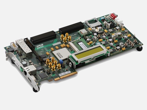
Key Takeaways
- Critical Power Sequencing: Properly ordered and stable power supply is essential for reliable FPGA operation.
- QSPI Boot Configuration: Accurate setup of boot modes and flash memory ensures successful bitstream loading.
- Comprehensive Validation: Rigorous timing and signal integrity checks prevent configuration failures.
1. Hardware Power-On Sequence
1.1 Power Supply Initialization
The power-on sequence for the Xilinx K7 FPGA is meticulously structured to ensure the device initializes correctly and operates reliably. Adhering to the recommended order minimizes current surges and stabilizes I/O states, which is crucial to prevent hardware damage and ensure predictable behavior.
Power Supply Sequence
| Step | Voltage Rail | Typical Voltage (V) | Tolerance |
|---|---|---|---|
| 1 | VCCINT | 1.0 | ±5% |
| 2 | VCCBRAM | 1.0 | ±5% |
| 3 | VCCAUX | 1.8 | ±5% |
| 4 | VCCAUX_IO | 1.8 | ±5% |
| 5 | VCCO | 1.0 - 1.8 | ±5% |
Power Supply Design Considerations
The power structure for 7-series FPGAs like the Kintex-7 is inherently complex. It is essential to control the power-on sequence using power management ICs that handle the EN (enable) and PGOOD (power good) signals. Ensuring that the power-on time meets Xilinx's specifications is critical for stable operation.
1.2 Reset and Initialization
After the initial power rails are applied, the PROG_B (program) pin plays a pivotal role in resetting the FPGA’s configuration logic. Holding PROG_B low ensures that any residual configuration data is cleared, providing a clean state for the new boot process.
Once all supply voltages are stable, PROG_B is released, allowing the FPGA to commence its configuration process. Some systems implement an external reset circuit to automatically manage the assertion and de-assertion of PROG_B based on power rail stability.
2. QSPI Boot Configuration Process
2.1 Boot Mode Selection
Selecting the correct boot mode is crucial for the FPGA to initiate the QSPI boot process. This involves configuring the mode-select pins (such as MODE[1:0]) to QSPI mode. Additionally, verifying that any jumpers or strap settings on the board align with QSPI boot requirements ensures the FPGA sources its configuration from the correct flash memory.
2.2 Flash Memory Initialization
With the boot mode set to QSPI, the FPGA begins interfacing with the external QSPI flash device post-reset. The flash memory must be properly powered and its chip-select signals correctly sequenced to facilitate seamless communication. The FPGA's internal configuration engine initializes the flash device, often transitioning into Quad SPI mode to enhance data transfer rates.
2.3 Programming the QSPI Flash
Programming the QSPI flash involves writing the necessary boot images that the FPGA will load upon power-up. This can be achieved through various methods:
-
Using U-Boot: Utilize U-Boot commands such as
sf probe,sf erase, andsf writeto program the flash. -
From Linux: Boot Linux via an alternative method, place the
boot.binfile on the file system, and employ theflashcputility frommtd-utilsfor flashing.
2.4 Creating Boot Images
The boot images are typically generated using the PetaLinux environment. This process involves creating QSPI_boot.bin images using Boot Image Format (BIF) attributes and the Bootgen tool. Ensuring that these images are correctly formatted and contain all necessary components is vital for successful booting.
2.5 Reading the Bitstream
Upon powering on, the FPGA issues read commands following the QSPI protocol to retrieve the configuration bitstream from the flash memory. In Quad SPI mode, data transfer occurs over four data lines, significantly speeding up the configuration process. The bitstream is clocked into the FPGA through dedicated configuration pins, and proper addressing ensures that the FPGA retrieves the correct segments of the bitstream.
2.6 Configuration Processing and Completion
As the bitstream is loaded, the FPGA's configuration logic parses and programs the internal SRAM, I/O configurations, and routing. Once the entire bitstream is successfully loaded and configured, the FPGA asserts the DONE signal, indicating that the configuration process is complete and the FPGA is ready to execute its configured logic.
3. Important Timing Considerations
3.1 Supply and Reset Timing
Adhering to the timing specifications outlined in the FPGA's datasheet is imperative. This includes ensuring that all supply voltages have sufficient time to stabilize before the configuration process begins and that the PROG_B signal is de-asserted only after power stability is achieved. Failure to meet these timing requirements can lead to incomplete or failed configurations.
3.2 Flash Access Timing
The interaction between the FPGA and the QSPI flash memory is governed by strict timing parameters. This includes the flash memory's read latency, the number of dummy cycles, and the timing for switching into Quad mode. Aligning the FPGA's configuration controller parameters with the flash memory's specifications is essential to maintain data integrity and ensure smooth bitstream retrieval.
3.3 QSPI Mode Switching
Transitioning the QSPI flash into Quad mode involves sending specific commands that enable four-bit data transfers. It is crucial to verify that the flash memory device supports these commands and that all relevant signals (IO0–IO3) are correctly routed and terminated to prevent communication errors.
4. Validation and Debugging
4.1 Verifying Power Rail Sequencing
Ensuring that the power rails follow the recommended sequencing is the first step in validation. Reviewing the board-level schematic to confirm voltage regulator sequencing and load conditions can preempt potential power-related issues.
4.2 Monitoring Configuration Process
Utilizing Xilinx configuration analysis tools such as the Vivado Hardware Manager or iMPACT utility allows for real-time monitoring of the configuration process. These tools can provide insights into the behavior of signals like PROG_B and DONE, aiding in identifying and resolving issues that arise during boot.
4.3 Signal Integrity Checks
Employing probes or onboard debug logic to examine the timing and integrity of key signals (e.g., flash interface signals) can help detect anomalies that might lead to configuration failures. Ensuring clean and stable signal transitions is fundamental to reliable FPGA operation.
5. Summary
Successfully booting a Xilinx K7 FPGA via QSPI involves a harmonious interplay between precise power sequencing, accurate boot configuration, and meticulous timing adherence. The process begins with applying the power rails in the specified order, followed by resetting the configuration logic through the PROG_B pin. Setting the boot mode to QSPI directs the FPGA to retrieve its configuration bitstream from the external flash memory. The configuration process is accelerated through Quad SPI mode, culminating in the FPGA asserting the DONE signal upon successful configuration.
Crucial to this entire process is the validation of power timing, flash access parameters, and signal integrity, all of which contribute to a robust and repeatable boot sequence. Adhering to these detailed steps ensures that the FPGA initializes correctly, operates reliably, and executes its configured logic as intended.
Conclusion
The detailed steps and considerations outlined for the Xilinx K7 QSPI boot process and hardware power-on sequence are vital for achieving reliable and efficient FPGA operation. By meticulously following the recommended power sequencing, accurately configuring boot modes, and adhering to stringent timing requirements, engineers can ensure seamless initialization and functioning of the FPGA. Comprehensive validation and debugging further enhance the robustness of the system, mitigating potential issues and facilitating smooth deployment in production environments.
References
 media.digikey.com
Last updated February 13, 2025