
Revolutionizing Chip Design with Reinforcement Learning
Unveiling how AI-driven methods optimize chip layouts and streamline design processes
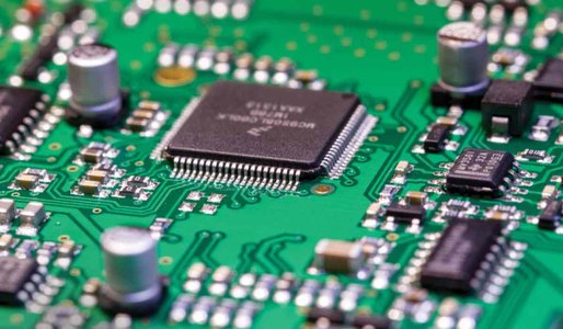
Highlights
- Automation and Efficiency: Reinforcement learning automates chip floorplanning and component placement, reducing design cycles dramatically.
- Optimization of PPA: RL techniques optimize power consumption, performance, and area (PPA) by learning optimal placement strategies from vast design data.
- Innovative Decision-Making: The RL agent iteratively refines its strategy through rewards, leading to superior designs that can outperform traditional methods.
Understanding Reinforcement Learning in Chip Design
Reinforcement learning (RL) has emerged as a pivotal technique in the field of chip design, introducing groundbreaking methods to automate and optimize tasks traditionally handled by human experts. At its core, RL leverages data, trial-and-error learning, and reward-based systems to guide an agent through complex decision spaces. In chip design, this means the RL agent learns how to strategically place circuit components to meet specific objectives such as minimizing power consumption, enhancing performance, and reducing the chip area.
Key Applications in Chip Design
Chip Floorplanning and Placement
One of the most critical factors in chip design is floorplanning—the arrangement of various circuit components on a chip. RL treats chip floorplanning as a sequential decision-making problem where every placement decision influences subsequent layout outcomes. For instance, systems like DeepMind’s AlphaChip have shown how RL can optimize the layout process by considering factors such as wire-length minimization, congestion reduction, and overall chip performance. Using a state representation (typically in the form of grids or graphs), the RL agent selects the placement for each component while receiving feedback (rewards) based on the quality of the design.
Arithmetic Circuit Design
Beyond standard floorplanning, reinforcement learning is also applied to more specialized tasks such as arithmetic circuit design. NVIDIA, for example, has used RL to develop optimized arithmetic circuits that are both smaller and faster than those designed using conventional electronic design automation (EDA) tools. By focusing on the intricate aspects of parallel prefix circuits and using deep neural networks to represent the policy and value functions, RL can explore and validate innovative design proposals that substantially improve the chip’s performance.
Optimization of Complex Design Parameters
Integrating RL into the chip design process permits co-optimization of multiple design parameters simultaneously. Instead of relying solely on fixed heuristics or traditional optimization algorithms, RL approaches explore a vast solution space where it can dynamically adjust to achieve optimal power, performance, and area (PPA) metrics. This process not only automates repetitive tasks but also reduces the overall design cycle from several years to weeks or even hours. The adaptability of RL allows engineers to focus on innovative design aspects, pushing the boundaries of chip efficiency and functionality.
Core Process and Methodologies
The application of RL in chip design follows a structured process that iteratively improves the design quality. This process typically involves:
1. Problem Formulation
The initial step involves defining the chip design task as an RL problem. Designers formalize the objectives (e.g., reducing power consumption or enlarging clock speeds) and set constraints, which then form the "environment" in which the RL agent operates. In most cases, chip layouts are represented as graphs or grids that capture the spatial relationships between components.
2. Training the RL Agent
Once the problem is defined, the RL agent is trained on historical design data. The agent experiments with different placement strategies and learns from the rewards it receives based on the quality of the resulting layout. Using advanced techniques such as deep reinforcement learning, the agent refines both its policy (the modus operandi for making decisions) and its value function (estimating the future rewards based on a given state), ensuring that each iteration progressively improves design efficiency.
3. Evaluation and Fine-Tuning
After training, the performance of the RL agent is rigorously evaluated against benchmark designs and human expert-designed layouts. Designs are assessed on several key attributes, including signal integrity, routing efficiency, and overall power-performance-area trade-offs. The process often involves iterative refinement, where unsuccessful strategies lead to adjustments and additional training, ensuring a reliable and effective chip design solution.
4. Real-World Implementation and Adaptability
One of the most compelling benefits of using RL in chip design is the adaptability to various architectures and design requirements. Whether it’s optimizing for minimal power consumption in mobile devices or maximizing processing speed in high-performance computing systems, the RL agent’s decision-making capabilities can be tuned to meet highly specific targets. This adaptability enhances the versatility of RL in addressing new challenges as chip technologies evolve.
Comparative Analysis: RL Versus Traditional Methods
Traditional optimization methods in chip design heavily rely on deterministic heuristics and exhaustive search techniques. These approaches, while effective, are often time-consuming and may not explore the full range of possible design adaptations due to their reliance on preset assumptions. In contrast, RL offers a dynamic and data-driven alternative capable of:
| Aspect | Traditional Methods | Reinforcement Learning |
|---|---|---|
| Automation | Manual design with human intervention. | Automated design processes with minimal human oversight. |
| Exploration | Limited to predefined heuristics and exhaustively searched solutions. | Dynamic exploration of vast design spaces based on cumulative learning. |
| Adaptability | Static methods that require manual adjustments for new scenarios. | Evolves with new data, adapting to different design requirements seamlessly. |
| Efficiency | Often slower with longer design cycles. | Significantly reduces cycle time, enabling expedited innovation. |
| Optimization | May not find global optimum due to heuristic limitations. | Learns to find near-optimal or optimal configurations through rewards. |
This table highlights the contrasting strengths of reinforcement learning compared to more conventional chip design methodologies. The ability of RL to learn from historical data and adapt to real-time feedback makes it especially suited for the rapidly evolving demands of modern semiconductor design.
Benefits and Impact on the Semiconductor Industry
Enhanced Performance and Power Efficiency
The utilization of reinforcement learning in chip design is already bearing significant fruit in terms of performance enhancement. By optimizing component placement, RL-based designs can achieve improved signal integrity and reduced power leakage. This not only meets the technical demands of high-performance computing but also addresses the increasing energy constraints in modern electronics.
Reduced Design Time and Cost
One of the revolutionary benefits of RL is the drastic reduction in design cycle time. By automating complex layout decisions, the need for extensive manual iterations and trial-and-error processes is minimized. This results in speeding up the design process from years to mere weeks or even hours, significantly reducing development costs and accelerating time-to-market for new chips.
Scalability and Flexibility
RL-based approaches are inherently scalable, allowing them to handle the increasing complexity of modern chip designs, which often involve millions or billions of components. Furthermore, their flexibility makes them adaptable to various chip architectures—from microcontrollers in household gadgets to high-end processors used in supercomputers—ensuring that the ever-growing requirements of the semiconductor industry are met efficiently.
Challenges and Future Directions
Current Challenges
Although reinforcement learning has demonstrated enormous potential in chip design, it also poses several challenges. The training process for RL agents typically requires large datasets of high-quality designs, which may not always be readily available. In addition, the complexity of chip design means that even small inaccuracies in state representation or reward mechanisms can lead to suboptimal results. Addressing these challenges requires ongoing research and innovation in modeling, simulation, and hybrid approaches that can combine RL with traditional optimization techniques.
Future Directions
The future of applying RL in chip design looks exceedingly promising. As computational resources and algorithmic techniques continue to improve, RL agents will likely become even more sophisticated, handling more aspects of the chip design process. There is considerable potential to integrate RL with model-based systems, where a simulated chip environment allows the agent to perform virtual experiments. Consequently, this could further reduce the time and resources required during the prototyping phase and allow designs to be iterated more rapidly. Furthermore, the advent of quantum computing and neuromorphic chips may open entirely new realms where RL can contribute to devising revolutionary design strategies, unlocking capabilities that traditional methods might not achieve.
References
- How AlphaChip Transformed Computer Chip Design - DeepMind
- Chip Design with Deep Reinforcement Learning - Google Research
- A Graph Placement Methodology for Fast Chip Design - Nature
- ArXiv Paper on RL in Chip Design - ArXiv
- Google Research Circuit Training - GitHub
Recommended Queries for Further Exploration

Last updated March 26, 2025