
Influence of Datapath Fanout on VLSI Design
Understanding Speed, Density, and Routing in Digital Circuits
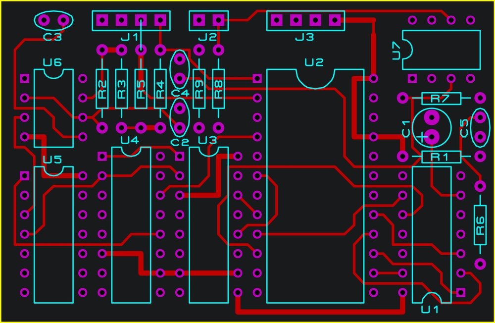
Key Highlights
- Speed Impact: Higher fanout increases capacitance and delays, while lower fanout supports faster transitions.
- Cell Density: Lower fanout allows for more compact cell arrangement; higher fanout may require additional buffers leading to increased area.
- Routing Complexity: High fanout raises routing congestion, whereas lower fanout simplifies interconnect routing.
Introduction to Datapath Fanout in VLSI
In digital circuit design, particularly in the context of Very Large Scale Integration (VLSI), datapath fanout is a critical parameter that defines the number of gate inputs driven by the output of a given logic component. This concept is central to understanding how signals propagate through a circuit, and it has direct ramifications on speed, standard cell density, and routing congestion.
The term "datapath fanout" encompasses the physical and electrical load presented by the subsequent gates a driver must power. The more devices a driver must connect to, the greater the cumulative load will be. This increased load manifests as additional capacitance, which in turn influences the delay of signal transitions through the circuit. This article explores how varying the number of outputs in a datapath affects key design trade-offs, including dynamic performance, physical layout constraints, and routing complexities.
Influence on Speed
High Datapath Fanout and Speed
When a datapath component such as a logic gate drives a large number of downstream components, a situation known as high fanout occurs. The primary implication of high fanout is the escalation of electrical load due to increased capacitance. Each connected gate's input adds capacitance to the load that the driving output needs to overcome during a transition from a low to high or high to low state. The overall effect is an increase in the propagation delay, which directly impacts the maximum operating frequency of the circuit. This delay is modeled by the RC (resistance-capacitance) time constant, where the equation is:
\( \text{\(Delay \propto R \times C\)} \)
Higher capacitance C means a longer charge/discharge time, leading to slower transitions. Designers may mitigate these delays by inserting buffering stages. However, this buffering increases power consumption and adds to the overall complexity.
Low Datapath Fanout and Speed
By contrast, a lower fanout reduces the overall capacitance seen by the driver. This enables quicker charging and discharging of the capacitive loads, thus shortening the delay associated with each signal transition. Faster signal propagation translates to improved frequency response and superior overall performance. Furthermore, circuits with lower fanout are more amenable to high-speed operation, as they do not suffer the delay penalties associated with the large capacitive loads inherent in high fanout scenarios.
Impact on Standard Cell Density
High Datapath Fanout and Standard Cell Density
Standard cell density refers to how tightly logic cells can be packed in a chip layout. In cases of high datapath fanout, additional buffers and driver replicas are often required to cope with the increased load. These extra cells take up valuable space, potentially lowering the overall cell density. Buffer insertion, while critical for maintaining signal integrity across large fanout networks, results in greater area overhead. This increased area usage can be a limiting factor in designs where space is at a premium. Moreover, during the placement phase, clustering of cells may occur to reduce wire lengths, which might further complicate efforts to achieve optimal density.
Low Datapath Fanout and Standard Cell Density
A lower fanout typically translates to fewer required buffers and minimal need for additional driving circuitry. This leads to a more compact layout where cells are packed more efficiently, bolstering standard cell density. The advantages of high density include reduced die size and hence a lower cost per chip, as well as potentially better thermal performance due to a more evenly distributed activity. However, designers must balance the reduced need for buffers with the possibility of underutilization of gate driving capacity.
Routing Congestion Considerations
Routing Challenges with High Datapath Fanout
Routing congestion is another critical factor affected by datapath fanout. In circumstances characterized by high fanout, a single driver must connect to numerous other cells. This produces a scenario where multiple interconnects converge to a single point, often leading to routing congestion. Congested routing can result in suboptimal wire lengths and may force the designer to use additional routing layers, which further complicates the circuitry layout. Increased routing complexity can sometimes result in timing uncertainties, making it more challenging to meet the design's performance specifications. Engineers may address these issues by duplicating drivers or using advanced routing algorithms, but such remedies contribute to increased design overhead and complexity.
Low Fanout and Simplified Routing
Lower fanout inherently reduces the complexity of the routing network. With fewer connections to manage, the interconnect architecture becomes more straightforward, leaving ample routing resources to achieve optimal wire layouts. This simplicity not only reduces likelihood of congestion but also supports cleaner and more predictable signal propagation. The resulting layout improvements facilitate easier timing optimizations and present fewer risks of routing-induced signal degradation.
Benefits and Impacts: A Comparative Analysis
The design trade-offs related to datapath fanout are multi-dimensional. Both high and low fanout configurations come with their respective benefits and potential drawbacks. Understanding these trade-offs is pivotal for circuit designers, as the maintenance of electrical integrity, performance, and efficient use of chip area requires careful planning and balancing.
Benefits and Impacts of Higher Datapath Fanout
Benefits:
- Simplified Logic Structure: High fanout can reduce the number of discrete logic levels by distributing a signal to multiple endpoints from a single source. This can simplify the overall logic structure and potentially reduce the number of required gate stages.
- Increased Functional Connectivity: By driving multiple inputs from one output, designers can achieve greater functional interconnectivity within the circuit, which might be beneficial in designs requiring parallel operations or where signal duplication is necessary.
Impacts:
- Increased Delays: The primary drawback of high fanout is the added capacitance which can slow down signal propagation significantly, thereby affecting circuit speed.
- Higher Power Consumption: Buffers and additional drivers that are necessary to manage high fanout conditions can increase power usage, which is a critical consideration in power-sensitive applications.
- Routing Congestion: With more loads connected, the routing resources are stressed, leading to potential routing congestion and increased interconnect wire lengths.
- Reduced Standard Cell Density: The need for extra buffers or duplicates takes up additional space, thereby potentially increasing the overall die size.
Benefits and Impacts of Lower Datapath Fanout
Benefits:
- Enhanced Speed: Lower fanout incurs reduced capacitance, which in turn accelerates signal propagation and supports high-frequency operation.
- Improved Cell Density: Fewer required buffers allow for more compact cell arrangements, resulting in optimal usage of the available chip area.
- Simplified Routing: With fewer connections to be routed from a single point, the physical interconnect layout is less congested, thereby enabling more straightforward and efficient routing.
- Reduced Power Consumption: As lower capacitance is involved, the overall power drawn for charging and discharging signals is minimized.
Impacts:
- Potential Complexity in Connectivity: While lower fanout benefits speed and density, it might restrict how many load connections a single output can support, thereby necessitating additional design techniques if more widespread connectivity is required.
- Increased Gate Count: To achieve required functionality when using lower fanout, designers might have to incorporate additional logic stages or replicate signals elsewhere, potentially increasing overall gate count under certain conditions.
Comparative Summary Table
| Aspect | High Datapath Fanout | Low Datapath Fanout |
|---|---|---|
| Speed | Increased capacitance leads to higher delays; may require buffers. | Lower capacitance supports faster signal transitions. |
| Standard Cell Density | Extra buffering may reduce density and increase die size. | Fewer buffers allow for a denser, more compact layout. |
| Routing Congestion | Multiple outputs create routing complexities and congestion. | Simpler and less congested routing due to fewer connections. |
| Power Consumption | Higher due to extra drivers and buffers required for heavy loads. | Lower power consumption because of reduced load capacitance. |
| Logic Connectivity | Can reach many endpoints from one source; useful for parallel processes. | May limit direct connectivity; sometimes requires replication. |
Design Considerations and Practical Implications
VLSI design is essentially a balancing act. The decision to implement a higher or lower datapath fanout configuration must consider various factors including speed requirements, area constraints, and the tolerable level of routing complexity. In scenarios where high-speed performance is paramount, designers often lean towards lower fanout designs complemented by efficient buffering and routing strategies. Conversely, in systems where extensive connectivity is necessary, higher fanout may be accepted, with additional mitigation steps to control delays and manage routing congestion.
In modern integrated circuit design, technological advancements also provide multiple techniques for balancing these trade-offs. For instance, the use of tapered buffers—a series of progressively sized buffers—can help manage the delay penalties associated with high fanout while still allowing widespread signal distribution. Additionally, advanced placement and routing algorithms can partly relieve the physical design challenges, optimally clustering and dispersing cells to minimize interference, congestion, and delay.
It is not uncommon for sophisticated design tools to analyze fanout effects during synthesis and physical layout stages, automatically adjusting the distribution of signals and buffers. This dynamic approach helps to optimize both the electrical performance and the physical area utilization. However, designers must remain vigilant to manual adjustments and fine-tuning, particularly in critical high-performance paths or when tight power budgets are allocated.
In-Depth Analysis of Trade-Offs
The precise influence of datapath fanout spans multiple dimensions of chip design. The overall speed of an integrated circuit is inversely proportional to both the physical capacitance that needs to be driven and the number of intermediary buffering stages inserted to manage that load. For digital systems operating at high frequencies, any incremental delay may push the design towards timing violations, necessitating a reevaluation of fanout strategy.
Similarly, cell density is directly affected by the need to incorporate additional driver circuits. While high density is desirable for reducing manufacturing costs and minimizing chip area, it can be compromised by the practical necessity of inserting buffers in high fanout networks. In this sense, the lower fanout approach naturally fits designs targeting high density, as the minimal requirement for buffering allows designers to pack standard cells more tightly.
Lastly, routing congestion must not be underestimated. The physical paths through which signals travel on a chip become increasingly complex with a high number of connections from a single source. This complexity requires more routing resources and often results in suboptimal signal paths, thereby increasing the overall delay and power consumption. In contrast, simpler routing associated with low fanout improves predictability in signal timing and often enhances the overall reliability of the design.
References
- Optimized Layout Techniques - UT Design Analysis
- Datapath Delay and Logic Levels - AMD Documentation
- High Fanout Net Optimization Techniques - AMD
- Placement and Congestion Insights - PhysicalDesign4U
- Standard vs High Density Fan-Out - Semiconductor Engineering
Recommended Further Queries
 mantravlsi.blogspot.com
Last updated March 10, 2025