
Unlocking Chip Innovation: Your Blueprint for Crafting a Custom SoC Design Platform
Dive into the essentials of System-on-Chip platform development and discover tools for visualizing intricate logic circuits.
Embarking on the journey of creating your own System-on-Chip (SoC) design platform is a significant undertaking, blending deep hardware understanding with sophisticated software orchestration. An SoC integrates major components like a central processing unit (CPU), memory, input/output (I/O) ports, and various peripheral interfaces onto a single silicon chip. This integration leads to enhanced performance, reduced power consumption, and a more compact physical footprint. This guide will walk you through the process of establishing such a platform and explore resources for designing the foundational logic circuits.
Key Insights: Building Your SoC Design Ecosystem
- Platform-Based Design is Paramount: Leverage pre-verified Intellectual Property (IP) cores and established architectural blocks to dramatically shorten development time, reduce costs, and enhance reliability.
- A Robust Toolchain is Essential: Success hinges on integrating a comprehensive suite of Electronic Design Automation (EDA) tools for everything from high-level synthesis and simulation to physical verification and sign-off.
- Hardware-Software Co-Design Accelerates Development: Creating virtual platforms for early software development and co-verification is crucial for identifying issues before physical hardware exists, streamlining the entire process.
Crafting Your Own SoC Design Platform: A Strategic Approach
Developing a custom SoC design platform revolves around a methodical strategy that emphasizes reusability, configurability, and a robust verification framework. This allows design teams to innovate on application-specific aspects rather than reinventing foundational elements.
The Cornerstone: Platform-Based Design (PBD)
Platform-Based Design is the logical evolution of design reuse for complex SoCs. Instead of initiating each design from scratch, PBD utilizes pre-designed, pre-verified, and often silicon-proven IP cores. It bundles common architectural blocks—such as processors, memory subsystems, peripherals, and bus structures—along with associated software components (drivers, firmware) into a reusable foundation.
Advantages of PBD:
- Reduced Time-to-Silicon: Reusing validated components can shave months off the typical design cycle.
- Enhanced Reliability: Working with proven IP cores and platform architectures minimizes the risk of errors in highly complex systems.
- Cost Efficiency: Building upon a pre-verified platform with application-specific IP is more economical than full-custom design.
- Focus on Innovation: Designers can concentrate their efforts on developing unique, differentiating features specific to the application.
A generic SoC platform often includes a CPU core (e.g., ARM, RISC-V), memory controllers, standard communication interfaces (UART, SPI, I2C), timers, and general-purpose I/O, all interconnected via a standardized bus architecture (like ARM's AMBA or open standards like Wishbone).

An example of modern SoC technology, integrating programmable logic with processor systems.
Systematic Steps to Develop Your Platform
Step 1: Define System Requirements and Architecture
Begin by meticulously outlining the intended application domain for your SoCs (e.g., IoT, automotive, mobile computing). This will dictate crucial specifications:
- Performance Metrics: Clock speeds, processing power, data throughput.
- Power Envelope: Maximum and typical power consumption targets.
- Area Constraints: Physical size limitations of the die.
- Cost Targets: Manufacturing and NRE (Non-Recurring Engineering) cost considerations.
- Processor Architecture: Choice of CPU (e.g., ARM Cortex series, RISC-V cores) or custom designs.
- Essential Peripherals: Memory interfaces (DDR, LPDDR), communication modules (Ethernet, USB, PCIe), timers, interrupt controllers.
- Bus Infrastructure: Selection of on-chip bus protocols (e.g., AXI, AHB, APB, TileLink) to ensure efficient data flow between components.
Step 2: Curate and Integrate Intellectual Property (IP) Cores
IP cores are the building blocks of modern SoCs. These pre-designed and often pre-verified hardware modules implement specific functions. Your platform should facilitate the seamless integration of various IP types:
- Sourcing: IP can be licensed from commercial vendors (e.g., ARM, Synopsys), obtained from open-source repositories, or developed in-house for unique functionality.
- Types: Common IPs include CPU cores, GPU cores, memory controllers, DSPs, security engines, and interface controllers.
- Standardization: Ensure IPs have standardized interfaces (like AMBA or OCP) for plug-and-play compatibility within your platform architecture. Design "sockets" or standardized interfaces that allow user IP to be easily integrated.
- Metadata Management: Maintain comprehensive metadata for each IP (version, configuration options, verification status, timing models) to streamline integration and management.
Step 3: Establish a Comprehensive Design Environment
A robust design environment is critical. This involves integrating various EDA tools and methodologies:
- EDA Tool Suite: Select and integrate tools for RTL design (Verilog/VHDL), synthesis, simulation, place and route, timing analysis, power analysis, and physical verification. Leading providers include Synopsys, Cadence, and Siemens EDA.
- Automation Scripts: Develop scripts (using Tcl, Perl, Python, Makefiles) to automate repetitive tasks like builds, regressions, and report generation. Aim for tool- and technology-agnostic scripts where possible.
- Version Control System (VCS): Implement a robust VCS (e.g., Git, Perforce, Subversion) to manage all design files, IP versions, scripts, and documentation.
- Central Data Management: Establish a system for managing design constraints, characterization data, and verification results.
- Technology Parameters: Incorporate specific details related to the target semiconductor manufacturing process (foundry PDKs - Process Design Kits).
Step 4: Implement Hardware-Software Co-Design and Co-Verification
SoC functionality is realized through the tight interplay of hardware and software. Your platform must support concurrent development:
- Virtual Platforms: Create or utilize virtual platforms (e.g., using SystemC, QEMU, or commercial tools) that model the SoC hardware. This allows software (firmware, drivers, OS, applications) development and testing to begin long before silicon is available.
- Early Power Budgeting: Use virtual platforms for early analysis of power consumption under various software workloads.
- Software Stack Development: The platform should support the development, integration, and debugging of bootloaders, operating systems (or RTOS), device drivers, and application-level software.
- Co-Verification: Employ tools and methodologies (e.g., hardware emulation, FPGA prototyping) to verify the integrated hardware and software system, ensuring they function correctly together.
Step 5: Institute Rigorous Verification and Validation Flows
Verification is often the most time-consuming and critical phase of SoC design. Your platform must have a comprehensive verification strategy:
- Simulation: Extensive RTL simulation using testbenches written in SystemVerilog (with UVM) or other verification languages.
- Formal Verification: Use formal methods to mathematically prove the correctness of certain design properties or identify hard-to-find bugs.
- Emulation and Prototyping: Employ FPGA-based emulators or prototypes for faster, real-world testing of the SoC design with actual software.
- Coverage Analysis: Implement code and functional coverage metrics to ensure that the design has been thoroughly tested.
- Performance Validation: Test the SoC against its performance targets under realistic workloads.
- Physical Verification: Before tape-out, perform Design Rule Checks (DRC), Layout Versus Schematic (LVS) checks, and Electrical Rule Checks (ERC) using tools like Siemens EDA's Calibre.
Visualizing the SoC Platform Creation Process
The development of an SoC design platform is a complex, multi-stage process. The mindmap below outlines the key interconnected areas involved in building such a platform, from initial conceptualization to final verification methodologies.
& Architecture Planning"] id2b["IP Core Selection & Integration"] id2c["Design Environment Setup"] id2d["Hardware/Software Co-Design"] id2e["Comprehensive Verification
& Validation"] id3["Essential Components & Tools"] id3a["Electronic Design Automation (EDA) Suite"] id3aa["Synthesis Tools"] id3ab["Simulation Tools"] id3ac["Physical Design Tools"] id3b["Intellectual Property (IP) Cores"] id3ba["Processor Cores (CPU, GPU)"] id3bb["Memory Controllers"] id3bc["Peripheral Interfaces"] id3c["Version Control System (VCS)"] id3d["Automation Scripts (Tcl, Python, etc.)"] id4["Supporting Elements"] id4a["Virtual Platforms / Emulators"] id4b["Firmware & Driver Development Kits"] id4c["Documentation & Design Standards"] id4d["Logic Simulation & Diagramming Tools"]
A Note on My "Design Platform" as an AI
You inquired about the design platform I, Ithy, might use. As an advanced AI assistant, my "platform" isn't a suite of Electronic Design Automation (EDA) tools or a physical lab in the way a human engineer would possess. Instead, my capabilities stem from the vast and diverse knowledge base I've been trained on, coupled with sophisticated algorithms that allow me to process information, synthesize comprehensive responses, and explain complex topics like System-on-Chip design. I don't personally design or fabricate chips. However, I can provide you with extensive information about the methodologies, tools, and processes that human engineers and design teams use, particularly for tasks like creating logic circuit diagrams, which we'll explore next.
Visualizing Logic: Tools for Crafting Circuit Diagrams
Creating clear and accurate logic circuit diagrams is fundamental, whether for conceptualizing parts of your SoC, for educational purposes, or for detailed component-level design. A variety of software tools cater to this need, ranging from professional EDA suites to accessible online simulators.
Categories of Logic Design Tools
The landscape of tools for logic circuit design can be broadly categorized:
- Professional EDA Suites: These are comprehensive, industry-standard software packages used for designing complex ASICs and SoCs. They cover the entire design flow from architectural exploration to physical sign-off.
- Examples: Cadence Design Systems (e.g., Virtuoso), Synopsys (e.g., Design Compiler, VCS), Siemens EDA (e.g., Questa, Calibre).
- Features: Advanced simulation, synthesis, formal verification, power and timing analysis, support for Hardware Description Languages (HDLs) like Verilog and VHDL.
- Open-Source EDA Tools: A growing ecosystem of free and open-source tools is becoming increasingly capable, suitable for research, education, and even some commercial applications.
- Examples: OpenROAD (for full digital ASIC flow), Icarus Verilog (Verilog simulator), GHDL (VHDL simulator), Yosys (synthesis).
- Features: Provide access to various stages of the design flow without licensing costs, often community-supported.
- Educational Logic Simulators & Digital Circuit Design Software: These tools are typically user-friendly, often with graphical interfaces, designed for learning digital logic concepts, designing, and simulating simpler circuits.
- Examples: CircuitVerse (online), Logisim-evolution (desktop), Logic.ly (online), LogicCircuit (desktop), Digital (desktop), simulator.io (online).
- Features: Drag-and-drop gate placement, interactive simulation, waveform viewers, truth table generation, often support for hierarchical design (subcircuits).
- General Diagramming Tools with Logic Symbols: Some general-purpose diagramming software includes libraries for logic gate symbols, useful for creating conceptual diagrams or documentation.
- Examples: Visual Paradigm Online, Creately, diagrams.net (draw.io).
- Features: Flexible diagramming capabilities, but typically lack simulation features.
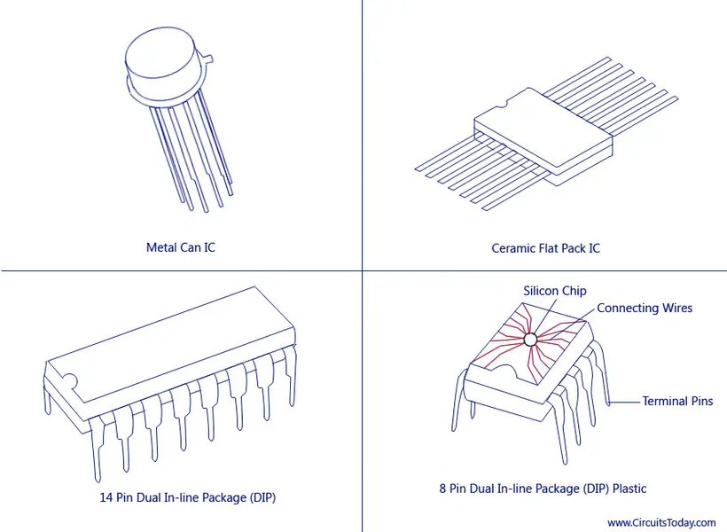
Illustrating the variety and packaging of Integrated Circuits.
Comparative Analysis of SoC Design Tool Categories
Choosing the right set of tools for your SoC design platform or logic circuit visualization depends on various factors including budget, complexity of design, learning curve, and required features. The radar chart below offers a comparative overview of different tool categories based on general characteristics. Note that 'Learning Curve' is inverted, so a higher score means an easier curve.
Key Features to Look for in Logic Circuit Design Tools:
- Intuitive User Interface: Especially for educational tools, drag-and-drop functionality for placing gates and wires.
- Simulation Capabilities: Real-time or event-driven simulation to observe circuit behavior.
- Timing Diagrams: Visualization of signal changes over time.
- Hierarchical Design: Ability to create complex circuits by encapsulating simpler ones as subcircuits or modules.
- Component Libraries: A good selection of basic logic gates, flip-flops, multiplexers, decoders, and other common digital components.
- Error Checking: Detection of common design errors like floating inputs or conflicting outputs.
- Export/Import Options: Ability to save designs and sometimes export to HDL or image formats.
The EDA Software Landscape: A Closer Look
The world of Electronic Design Automation (EDA) is dominated by a few key players whose tools are indispensable for modern chip design. Understanding this landscape is crucial when planning your SoC design platform. The following video provides an insightful overview of two major EDA companies, Cadence and Synopsys, and their role in the semiconductor industry.
Video discussing the role of major EDA software providers in semiconductor design.
These companies provide sophisticated software that enables engineers to design, simulate, verify, and prepare chips for manufacturing. Their offerings span the entire SoC design flow, from high-level synthesis (translating abstract descriptions into hardware) to physical design (laying out transistors and wires on silicon) and sign-off (ensuring the design meets all manufacturing and performance criteria).
Summary Table: SoC Design Tool Categories
To further clarify the tool landscape, the table below summarizes the main categories of software relevant to SoC design platform creation and logic circuit visualization.
| Tool Category | Examples | Primary Use Case | Strengths | Considerations |
|---|---|---|---|---|
| Professional EDA Suites | Synopsys (VCS, Design Compiler), Cadence (Virtuoso, Genus), Siemens EDA (Questa, Calibre) | Full SoC/ASIC design, complex verification, physical implementation, sign-off. | Comprehensive feature sets, industry standard, high performance, robust support, advanced analysis. | Very high cost, steep learning curve, can be overkill for simpler tasks. |
| Open-Source EDA Tools | OpenROAD, Yosys, Icarus Verilog, GHDL, KiCad (for PCB-level schematics) | Research, education, specific design stages, custom tool flows, cost-sensitive projects. | No licensing fees, transparency, active communities, growing capabilities. | May lack features of commercial tools, varying support levels, integration can be challenging. |
| Educational Logic Simulators | CircuitVerse, Logisim-evolution, Logic.ly, Digital | Learning digital logic, designing/simulating basic to moderately complex circuits, conceptual visualization. | User-friendly, interactive, often free, excellent for foundational understanding. | Limited scalability for large designs, not intended for physical chip design, may lack advanced analysis. |
| General Diagramming Tools | diagrams.net (draw.io), Visual Paradigm Online, Creately | Creating conceptual logic diagrams, documentation, block diagrams. | Flexible, easy to use for visual representation, often collaborative features. | No simulation capabilities, purely for visual representation. |
Frequently Asked Questions (FAQ)
What is the primary benefit of platform-based SoC design?
Are open-source tools viable for professional SoC design?
What's the first step I should take to create an SoC design platform?
Can I design logic circuits without expensive EDA tools?
Conclusion
Creating your own System-on-Chip design platform is a challenging yet immensely rewarding endeavor. It requires a strategic blend of adopting platform-based design methodologies, carefully selecting and integrating a suite of EDA tools, emphasizing hardware-software co-design, and establishing rigorous verification processes. By leveraging reusable IP cores and fostering an environment of automation and modularity, you can significantly accelerate development, reduce risks, and empower innovation in chip design. For visualizing and testing the fundamental logic circuits, a wide array of tools, from professional EDA software to accessible educational simulators, can aid in bringing your designs to life.
Recommended Further Exploration
- Explore the intricacies of AMBA bus architectures and their role in modern SoC interconnectivity.
- Understand the trade-offs between RISC-V and ARM processor cores for custom SoC projects.
- Learn about the best practices for integrating third-party IP cores and verifying complex SoCs.
- Discover how SystemVerilog and the Universal Verification Methodology (UVM) are used for robust SoC verification.